This thread has been locked.

If you have a related question, please click the "Ask a related question" button in the top right corner. The newly created question will be automatically linked to this question.

TPS543B25: TPS543B25 how to increase gain

Part Number: TPS543B25

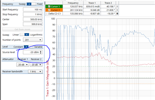
TPS543B25 chip how to increase gain ?the file include BODE image, Question is the gain passes through the  cross-over frequency and the waveform becomes flat. .TPS543B25 LOOP.docx

  • Hi Darren,

    Could you help translate to english version and upload it again so that our team could take look at it.

    Han, FAE

  • With the internally compensated devices, the only knobs are the ramp setting, output L and output C and the Cff in the feedback loop. 

    Since, the 220nH give phase and 330nH gives gain margin, has 250nH to 270nH been tested to check gain and phase.   

    The control loop will be stable with > 45 degrees phase margin. 

  • Hi David,

    Thanks for your support! My customer is actually talking about the gain margin. the requirement is >10dB of gain margin. we are wondering why it looks like a right-half zero after the crossover frequency - gain become flat and phase decreases a lot? Or you think it's actually a left half plane zero.

    It looks like the cross over frequency is a little bit high, do you think it might work to decrease the cross over frequency? How do you suggest on L/C/ramp changing.

    THanks,

    Han 

  • Test results 2 and 3 look good to me.    Test results for case 1 looks suspect and looks like a measurement or setup error.   the phase drops after 140kHz so quickly that it does not appear to be the control loop.    A pole should have a total of -90 degrees shift over 2 decades.   Double pole -180 degrees over 2 decades.  

    I see a shift of 50 degrees from 140kHz to 380kHz which can not be real.    I would retake this data and check the sw node and make sure during this measurement the sw node has jitter but is not experiencing a max duty cycle, or min on time or triggering current limit. 

    If the injection signal is too large, and causes the minimum on time or current limit to control the loop then the measurement is not meaningful.  

    Also, if the injection signal is too small, the test instrument can have a difficulty differentiating the signal from noise. 

  • if use TPS543B25,when i test LOOP , if output voltage is 0.8V to 1.4V  the source level of loop device  how to set ?Set how much is appropriate ? imy set  is -15dBm

  • The source level is not a universal setting that will work in all systems, pcb layout and bom are different etc. 

    My experience has been that experimenting with the levels and placement of the receiver ground connections (quiet ground) is needed to yield good results. 

    When injecting into the loop, monitor the sw node.   The sw node should have jitter but not reach the any of the limits: hs or ls current limits, on time, off time, duty cycle, etc when injecting signal and to obtain good results.    

    In the image, the source level selected is constant.   The constant setting will inject a fixed level across the frequency range.

    Consider using the variable setting.     With the variable setting, a shaped level can be defined.    The shaped level allows for setting the output level across the frequency.     I have had success will larger signal at low frequency (3dB at 100Hz) and smaller (-24db at 100kHz) at the higher frequencies.    Additionally, on some boards, I have had to use a 10:1 attenuator on the injection signal to get results.