This thread has been locked.

If you have a related question, please click the "Ask a related question" button in the top right corner. The newly created question will be automatically linked to this question.

LM5176: LM5176

Part Number: LM5176
Other Parts Discussed in Thread: CSD19532Q5B, UCC27714, CSD18540Q5B

Dear TI Team,

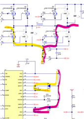
We are using LM5176 for our one of application.

We would like to understand below few queries 

1) Could you please clarify us, will the Higher side MOSFET ( HDRV1 Or HDRV2) will continue remain ON ( e.g 100% duty )?

Considering any case e.g boost, buck or any other mode.

2) If yes, how the boot capacitor will charge when upper MOSFET continue (100 %) ON e.g LO remain off?

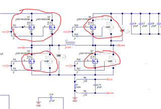
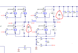
3) Will the LM 5176 can drive parallel  MOSFET topology i.e 4 or 5 MOSFETs are in parallel to increase the current capacity.

We are using CSD19532Q5B this MOSFETs for parallel topology.

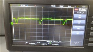
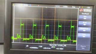
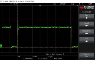
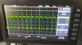
4) Could you please share few waveforms with us as below.

   i) HDRV1 & LDRV1 waveform for all modes ( e.g buck, boost any others mode)

  ii) HDRV2 & LDRV2 waveform for all modes ( e.g buck, boost any others mode)

 iii) Current sense ( i.e CS and CSG ) waveform for all modes ( e.g buck, boost any others mode).

Note: We checked in EVM details but we haven't found above waveforms in the same, so could you please share the same.

Thank you!

  • Hi Shankar,

    thank you for using the E2E forum.

    To your questions:

    1) Yes, the LM5176 does support 100% duty cycle.

    2) once the charge of the Boot Cap gets to low a recharge cycle will be added in-between

    3) yes, the LM5176 can drive parallel MOSFETs - for the number of MOSFETs in parallel please consider the drive capabilities of the gate driver and the gate charge of the used MOSFETs

    4) sorry I only have the waveforms available which are shown in the Datasheet and EVM users Guide.
    Perhaps you can just take one of the EVMs and capture the required waveforms there.

    Best regards,

     Stefan

  • Hi Stefan,
    Thanks for your support.

    1) Okay noted.
    2) Could you please explain how the recharge cycle path will be added in-between? And how will be the exact path for boot cap for recharging (Specially at 100% duty)? 
    3) Thanks to this, so considering this, Is it correct our understanding that the max output current ( let's say 60A to 80A) will be depend on only external mosfet & inductor considering driver capability of LM5176?
    4) okay noted.
    5) Like we mentioned, we are planning to use CSD19532Q5B this mosfets in parallel (let say 5 or 6 in parallel) could you please confirm is the LM5176 can drive this? 

  • Hi Shankar,

    there are two things to consider

    1. LDO drive capability to supply gate drivers:

    I_Gate = f_SW  (Qg)

    Qg (CSD19532) = 44nC   (max at 7V gate voltage)

    I _Gate  [300kHz) =  13.2mA

    2 MSOFET Switch at on clock cycle so a average current of 26.4.2mA will be needed by 1 MOSFET (no parallel)

    Current limit of LDO is 65mA -> 2 MOSFET in Parallel can be supplied by  LDO

    2. Gate drive strength

    Driver peak source current = 1.8A

    Qg = I * t

    t = 24 ns transition time <- this needs to be scaled by the number of MOSFETs in parallel - so transition time will get higher and therefore also transition losses.

    So if you need to have more then 2 MOSFETs in parallel you should use an external driver or use a multiphase design.

    Best regards,

     Stefan

  • Thanks Stefan for this.
    Well noted on your reply.

    Considering this, we are using external driver ( UCC27714) to drive the parallel mosfet ( 5 or 6).
    Could you please confirm 
    1) Is the UCC27714 & LM5176 combination suitable? ( considering all the cases e.g 100% duty, boost, buck etc)
    2) Also please let us know UCC27714 is suitable for 5 or 6 mosfet drive capacity ( please consider same MOSFETS CSD19532Q5B )

  • Hi Shankar,

    the driver needs to support 100% duty cycle.

    The external driver does not belong to our team. Maybe you can start a new thread asking that question so that the corresponding team can pick up.

    Best regards,

     Stefan

  • Hi Stefan
    Okay noted.

    1) In LM5716, Could you please explain how the recharge cycle path will be added in-between? And how will be the exact path for boot cap for recharging (Specially at 100% duty)?  with some diagram which show the path during 100%.

    2)  Is it correct our understanding that the max output current ( let's say 60A to 80A) will be depend on only external mosfet & inductor considering driver capability of LM5176?


  • Hi Shankar,

    1.

    sorry I do not have an diagram available showing the recharge in more detail.

    So let me describe in words. Assuming you are in Boost mode, the high side BUCK MOSFET is 100% on.

    If the Boot Voltage on the BUCK side goes below the threshold a special cycle on BUCK side will be added inbetween to recharge the Boot Cap on BUCK side

    2. 

    yes, this is correct.

    Best regards,

     Stefan

  • Thanks Stefan for your reply.

    1 => Okay noted, It is also okay if could you draw a diagram on any paper and show the path.
    Also as you mentioned, a special cycle will be added ( what is its max time duration and its adding frequency) .

    2. Thanks for confirm on this max current.

  • Hi Shankar,

    hope this helps (shows the path to charge Boot1 and Boot2 cap:

    As mentioned the it will recharge once the voltage gets below a certain level, so is defined by the leakage esp. of the Boot Cap an  the MOSFET gate.

    Best regards,

     Stefan

  • Hi Stefan,
    This is in continuous with above mentioned same system. 
    We are seen this abnormal waveform on SW1 & SW2 at 25A load but could not see this phenomenon till 23A.

    What could be the reason?
    SW2 wavform:
      

    SW1 waveform;

  • Hi Shankar,

    can you probe SW1, SW2 and VIN in one plot.

    Best regards,

     Stefan

  • Hi Stefan,
    We tried, but the issue is that when we trying to take SW1, SW2 & VIN etc on same graph then IC getting damages hence we took separately.
     

  • Hi Shankar,

    this is very confusing and also make no sense for me.

    I also look like the last scope plot above is negated - can you please check you connection points and the polarity.

    Best regards,

     Stefan

  • Hi Stefan,
    To avoid confusion, let's ignore above. At least can you check below SW1 & SW2 waveform.

    SW1 waveform above 23A load


    SW2 waveform above 23A load


    Q1: Could you confirm what is the reason for ringing on SW2
    above 23A load and same circuit with 20A load load there is no ringing on the SW2.

    Q2: Importantly Audio sound.
    Above 23A load, there is some audio sound ( tik-tik tik....) and above SW1,SW2 waveform observered.
    FYI we increased CBOOT to 1uF from 470nF till same issue facing.


  • Hi Shankar,

    Q1:

    The ringing looks like an overshoot due to parasitcs on the boards.

    There are several options to improve on that:

    - first of all the layout has an huge impact on that

    - adding a gate resistor to slow down the switching speed (Gate resistors are typically in the range of 1 to 10 Ohm)

    - adding a snubber - see also https://www.ti.com/lit/ta/ssztbc7/ssztbc7.pdf

    - adding a Diode parallel to the Body diode of the MOSFET

    Further info:

    https://www.ti.com/lit/an/slyt465/slyt465.pdf

    https://www.ti.com/lit/an/slva255/slva255.pdf

    https://www.ti.com/lit/an/slpa010/slpa010.pdf

    Q2:

    the Audio can be triggered from the overshoot.

    This are generated by either the inductor or the ceramic caps. To find out what is the source a  good method is to connect the inductor with some short flexible wires and move it off the board. If the noise is gone this is by the inductor if not it is most properly from some capacitors.

    Best regards,

     Stefan

  • Hi TI team,

    Could you please let us know.

    Q1: For LM5176, When VIN 24, VOUT 12V ( Buck mode)

     HDRV1 => Will it be 50% duty?

    HDRV2 => will it be 0% duty (Current flow via MOSFET body diode)?

    Is this our understanding correct?

    Q2: What will the voltage between HO wrt com pin for HDRV2 for above VIN and VOUT case?

    Q3: Also as load current increases, will the any impact on HDRV1 & HDRV2 duty % value?

    Q4: Q1,Q2 & Q3 repeat for VIN6V and VOUT 12V ( Boost Mode)?

  • HI Shankar,

    answer are mapped to your questions

    Q1:

      HDRV1 : 50%

      HDRV2 : 100% ( to avoid current through body diode as this generates high losses,  except during Softstart)   

    Q2 + Q4:

    will be 0V or VCC relative to SW (depending if the MSOFET is on or off

    Q3 +Q4: 

    not in static mode only during the transition - duty cycle depends on input and output voltage

    Q4 - Q1:

      HDRV1 : 100%

      HDRV2 : 50% 

    Best regards,

     Stefan

  • Hi Stefan,
    After all these issue, finally we decided to use TI LM5176 EVM board for testing purpose and we observed below spike issue.

    We kept same components as TI EVM suggestion but with two mosfets CSD18540Q5B (at each side Q2,Q3,Q4,Q5,Q6,Q7 & Q8 all are mounted) in parallel for higher current.


    Below is the SW1 waveform at 17V input and output is 12V.


    +Ve spike voltage was ~26V from above waveform
    -Ve Spike voltage was ~-3.5V from above waveform


    FYI:

    1) To reduce this spikes we added snubber 
       i) R=> 3R3, C=> 4n7
       ii) R=> 4R7, C=3n3

    2) Also tried with increasing gate resistance 0 to 10 Ohm 

    3) Also tried with adding diode D1 & D2 (SS220LWHRVG) to improve this spike but there is not improvement after adding this.


    After all these trial, above is the best waveform we had achieved. 

    Q1: Could you please do let us know how we can reduce this +Ve and -Ve side spikes?
    Q2: What is max -ve spike voltage at SW1 point that can sustain LM5176 ?


  • Hi Shankar,

    What was the input output voltage and load current during this test?

    Can you please zoom in to see the overshoot ringing/ waveform of falling and rising edge.

    Can you please share a photo which shows how you have attached the probes.

    Best regards,

     Stefan