This thread has been locked.

If you have a related question, please click the "Ask a related question" button in the top right corner. The newly created question will be automatically linked to this question.

TPSM53602: Input and output capacitance requirement

Part Number: TPSM53602
Other Parts Discussed in Thread: TPSM53604, TPSM33625, TLVM23625

Hi,

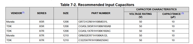
I'm planning on using TPSM53602RDAR. The datasheet clearly states requirements for both input and output capacitance, output capacitance as a function of output voltage and input capacitance 20uF ceramic.

  1. What constraints are considered when setting the output capacitance requirement? 42uF is rather huge and one of the main advantages of switching at high frequency like this device is being able to save in passives. 
  2. What constraints are considered when setting the input capacitance requirement? 20uF is rather huge and one of the main advantages of switching at high frequency like this device is being able to save in passives, additionally, in 8.2 Typical apllication, 2x 10uF 50V caps are used, it is not hard to find caps with 80% bias derating at 24V and so it makes me wonder whether the 20uF requirement is to be considered. Often the Cin in a buck converter is set by constraining the maximum input voltage variation, and by knowing fsw, i and C it can be calculated. I also performed a design in Webench and it recommended a total input capacitance after DC bias derating of 11uF.

THanks and regards

  • Hi Nicolas,

    The EVM for TPSM53602  only uses 2 * 10uF before derating, and that should be ok for your application. Additionally the COUT is 44uF, but it's designed for the worse case scenario of largest output voltage + highest current. You may be able to get away with less.

    TPSM53602 is a differently current trimmed design of the TPSM53604 which also requires 20uF of capacitance, but also allows 4A of output current. We are kind of limited by the inductor chosen for this corner case application (4A 36Vin). You can probably away with lower input capacitance, (TPSM33625 only requires 4.7uF + 0.1uF input C and uses 2 * 22uF for COUT).

    Also TPSM33625/TLVM23625 may be better for your design as those parts don't require as much capacitance in general, and you can set FSW to 2.2MHz. However, they have a little bit lower efficiency than the TPSM53602.

    Thanks,

    Andrew

  • Hi Andrew, thanks for your reply. I'm afraid I will need more information to address my design.

    Indicating the capacitance before derating is not very accurate given that different components will derate different. Can you confirm that the input capacitance can be calculated as in a generic buck by setting a voltage sag variation due to the current provided by the capacitor, i.e. Q = C * V; C = Q / V. Q is the integral of current wrt time, the squarewave-ish current provided by the input capacitor and the time, is the time during which the high side mosfet is on, then for calculating Cin = input_current * Tsw * duty / Delta_Vin.

    Regarding the Cout, the output voltage ripple is: DeltaVout = DeltaiL * Tsw / (8 * Cout)

    Then I don't get how it depends on output current and voltage... Is it related to the regulation? An expression where the designer is able to choose a compromise would be better.

    Thanks and regards

  • Hi Nicolas,

    Modules are a bit more rigid in terms of design freedom because of how the inductor and mosfets are already chosen for you. There isn't as much freedom as you think there is because of this. For these devices we want them to be as simple as possible which is why we provide a chart with values already populated.

    This particular design works optimally if 2 * 10uF capacitors with voltage rated to twice the voltage used. It's ok if they derate a little bit as shown in the webbench.

    If you aren't sure what capacitors you would like to use because they derrate differently, there's a list here that can help you with component selection:

    Another thing to consider is that the design takes advantage of symmetry so the magnetic field generated by current Cin to the TPSM53602, and the current from the TPSM53602  to COUT partially cancel out to get better radiated EMI.

    If you would like to experiment with optimizing COUT for your design, I highly recommend ordering an EVM and playing around with the values in order to get it to work.

    https://www.ti.com/tool/TPSM53602EVM

    Thanks,

    Andrew

  • Hi Andrew,

    How does inductance/MOSFET affect input capacitor...? Of course the input capacitor current will be equal to the inductor current while the high side switch is conducting but you still have one degree of freedom being input voltage ripple when choosing the input capacitance, thus why "There isn't as much freedom as you think there is because of this."...?

    The current waveforms in the input capacitor and output capacitor are not equal (squarewave vs triangular wave) thus there will be no magnetic field cancellation...

    I understand that this product is intended to simplify the design process for the customer but it would be great to also allow the integrator using this system in a less constrained configuration by explaining the constraints on choosing Cin and Cout.

    Regards

  • Hi Nicolas,

    The way this device was designed it has poor phase margin unless you put a bunch of capacitors on COUT. You can see this if you try to simulate a load transient on Webbench with insufficient COUT. I understand your frustration on why there's no calculator, but that's just how this device functions. If you use this device I highly recommend using the recommended values.

    The best advice I can give you is that if you would like to see what happens under your system's conditions with your selected capacitor configuration to our part I recommend simulating the circuit with Webbench or PSPICE.

    In Webbench you can select capacitor values in the menu like this.

    With regards to input output capacitor placement symmetry, there's symmetry along the x-axis. Every bit helps when you are trying to minimize EMI.

    Thanks,

    Andrew