This thread has been locked.

If you have a related question, please click the "Ask a related question" button in the top right corner. The newly created question will be automatically linked to this question.

LM5141: Please review the schematic.

Part Number: LM5141
Other Parts Discussed in Thread: AM62A7, SK-AM62A-LP, LM25141, CSD18563Q5A

Dear TI experts,

My customer using LM5141 to operate AM62A7.

They designed their schematic based on SK-AM62A-LP EVM schematic.

And they had no problem when they tested 1st sample, but the problem appeared when they tested 2nd sample.

- If they apply the input voltage from 12V to 48V, LM5141 works well.

- but if they apply the input voltage 48V directly, LM5141 died and no output is detected.

- They used power supply for input voltage.

- Finally they want to use 48V input voltage.

- current consumption is 100mA when input voltage is 12V, and 25mA when input voltage is 48V.

So I want you to review their schematic. I attach the 1st sample's schematic(rev.a) and 2nd sample's schematic(rev.B)

LM5141_SCH.zip

The changes from rev.A to rev.B are as below;

- D4 and TNR2 are not inserted.

- rated voltage of D3 is increased. (compared to rev.A)

- 4 PCS of Bead is changed to higher spec. (DC resistance/impedance is down, rated current is up)

- 100uF tantal capacitor has higher rated voltage. (62V to 100V)

- changed location of R58 and C18 (connected to pin 20)

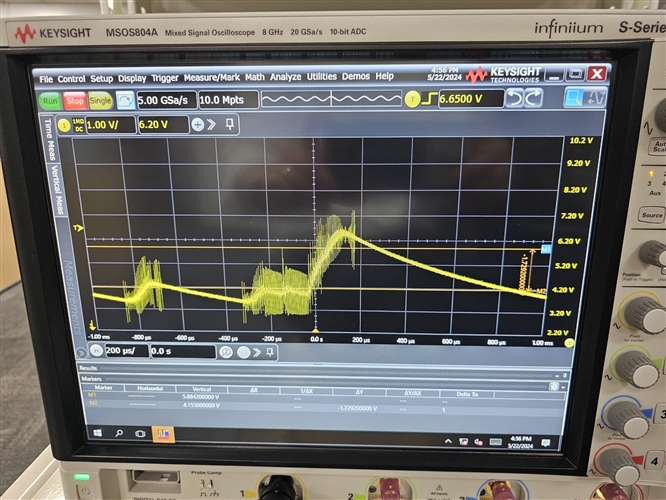
And below image is the waveform when my customer applies 18V input voltage to LM5141 and cut off input voltage.

As you see, the output is not stable. Could you check the reaon and find the way for stable output?

Best regards,

Chase

  • Hi Chase,

    Go ahead and send a completed quickstart file for this design, so we can review component selection, power loss and stability. What is C7 100uF electrolytic from VIN to VCCX pin 16 of the IC? VCCX is normally powered by a 5V rail. Note the input caps (across the FETs) need to be ceramics, e.g. 4.7uF/100V/1210.

    Regards,

    Tim

  • PS: I think C7 is a schematic error. As Vout = 12V, just go ahead and tie VCCX to GND if a 5V bias supply is not available.

    In general, tantalum caps connected across the input are not recommended given their failure modes and vulnerability to high dv/dt. As mentioned above, use ceramic caps across the FETs (see app note SNVA803 for correct layout placement). For EMI filtering, use an input filter inductor along with a suitable damping circuit as needed.

  • Hello, Timothy.

    I am the customer Mr. Jeong mentioned.
    I have a question following your answers.

    Q1. To be specific for our requirment of Buck(LM5141),
    Target input V is 48 and the range is min 12V ~ 65V.
    Output power requirment is that Vout is 5V, Iout is 5A(including enough margin).
    However, actuall current consumption is expected below 2A.
    So, I don't understand your expression "As Vout =12V, ......".
    Where it come out?

    Q2. In according to the excel "DESIGN-CALC" linked by you, Max Vin condition(65V) appeared by red letters when I enter the value.
    What is this exactly meaning?
    Does the buck not ensure the performance with the Max Vin? or other meaning?

    Q3. In your PS, the sentence "C7 is a schematic error" means that C7 is not grounded at lower side?
    In our first design(Rev.A), it was mistake and we recognized.
    We have debugged it physically on Rev.A.
    Also Rev.B schematic is corrected.
    In Rev.B circuit, lower side of C7, right side of C6, Pin VCCX are the same net as ground.
    Is this right?

  • Send on the quickstart calculator file so I can understand the circuit parameters. I thought I saw a 12V output mentioned in the schematic.

  • LM25141-Q1_quickstart_calculator_revA5_240524_2.xlsm

    There is no 12V output mentioned in the schematic.

    I attached the excel related with Q2.

    Also, you don't answer about Q3.

    Answer again Q2 and Q3 please.

  • And also I have more question.
    As Mr. Jeong mentioned, LM5141 often died when debugging.
    I thought I don't insert input voltage as much as its operating condition.
    I measured the input voltage waveform that didn't look exceed more than 60V when the moment of input skyrockets in case of applying the Vin 48V directly.
    But, the buck always dies even though it seems not over maximum rating.

    So, I wonder whatever conditions of buck dead.
    I don't understand why and I want to understand the circomstance.
    Please answer this certainly.

    Regard

  • Hello Chase,

    Sorry for the delay, Tim will provide an update within 24 hours.

    Thanks.

    David.

  • Hi Hogyun,

    Q2. I'm unable to download the file - try attaching it again. If you entered 65V for Vin-max, please ensure you're using the LM5141 quickstart calculator and not that for the LM25141 (as the filename suggests).

    Q3. Yes, the VCCX pin should be tied to GND if an external bias supply is not used. However, Vout = 5V here, so you can tie the output to the VCCX pin to reduce bias current taken from VIN.

    Here are additional notes:

    1. Given the 52V (max) to 5V conversion (10% duty cycle), a lower capacitance, higher Rdson FET is suitable for the high-side position. Take a look at the CSD18563Q5A for example (this could be used in both positions, as it also has lower Qrr).
    2. Input caps near the FETs should be ceramics, e.g. 4.7uF/100V/1210.
    3. No need for the 0Ω between AGND and PGND. Just connect the respective pins at the DAP.
    4. Crossover frequency should be designed to 10-12% of Fsw (this gives margin at hold/cold when the effective ceramic output capacitance decreases). 20% of Fsw is the abs max for crossover.
    5. Consider adding an RC filter on the current sense lines (if noise is suspected).

    Regards,

    Tim