Because of the Thanksgiving holiday in the U.S., TI E2E™ design support forum responses may be delayed from November 25 through December 2. Thank you for your patience.

This thread has been locked.

If you have a related question, please click the "Ask a related question" button in the top right corner. The newly created question will be automatically linked to this question.

TPS543B22: design issues

Part Number: TPS543B22

Tool/software:

Hi Team,

I want to actually use TPS543B22 in my design.
Vout:1V、Iout:10A

I have some questions I would like to ask

Q1: Regarding the EN Pin, I saw that the maximum voltage is 5.5V, but I accidentally connected 17V and found that it worked normally and the IC was not burned.
I know this design is not correct, but I want to know whether there are protected Diodes inside the EN Pin?
Because I measured the voltage of the EN Pin and found that the EN Pin voltage is maintained at 11.7V, and the same result is obtained when Vin is between 12 and 18V.

Q2: There is an OPA inside the EN Pin. What is the voltage source of this OPA? What is the voltage level of OPA -?
I would like to know if the 11.7V of Q1 is related to the internal OPA?

Q3: For the selection of Output Capacitor, I saw that P24. provides four ways to consider Cout.
Which of these are more recommended? Or can I choose any one?

Q4: There is a 10R between SW and FB. I saw that the description of this resistor is a measurement BODE diagram. Is it possible to remove this resistor and would it have any impact on the design?

Q5: On the FB feedback path, CFF and RFBT need to be installed. Refer to the public version of the design RFBT=10K, CFF=68pF. Suppose I modify RFBT=4.99K here, is it feasible to maintain CFF at 68pF?
Is there any formula I can use to verify the stability of this circuit?

Many thanks.

  • Q1 and Q2:   A one time test, does not equate to the circuit working for a long duration.  The abs max is 5.5V for EN.   There is an internal supply generated from VIN that pre-powers enable circuits and the pull up is derived from VIN. 

    Q3:  Use all of the Co equations, steady state ripple, load transient, unload transient and the stability are the specs that are used to estimate the Cout.

    Q4:  You can remove the 10ohm, but how will you verify the frequency response with an analyzer.

    Q5:  There is a simplis model on the product folder that can be use to check  frequency response.   Following the design procedure in datasheet or using webench from the bottom of the product folder at ti.com. If RFBT or the Lo or Cout values changes the cff may need to be adjusted.

    Since you are needing a 1V, copy the app circuit, this is the evm design and application circuit design.      

  • Hi,David

    I'm sorry that I forgot to reply to you. Regarding Q4, measuring frequency response may not be used in my design, so I am thinking about whether it can be removed? Will there be any functional problems after removing it?

    ---

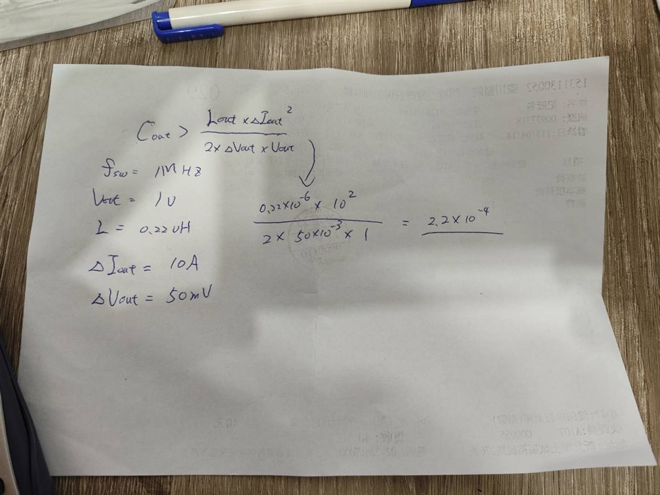
    To bother you again, I want to ask about the part of 7.2.1.2.4 Output Capacitor.
    In the formula of Equation 21, I saw that the calculation is related to the inductance, but I found that after I entered the numbers in this example, I could not calculate 91uF.
    I would like to ask, which value is wrong?

    thanks for your reply

  • The consequence of removing the 10 ohm in feedback path is that you will not be able to test the frequency response. 

    Eq 21 the result is a typo, your calculations are correct

    Best, 

    David