Other Parts Discussed in Thread: TPS62870, TPS62869, TPS62870-Q1,
Tool/software:
In design phase of an ASIC validation test board and considering the TPS62874 for the core voltage regulator. Application is 3.3 VIN, 0.5-0.55 VOUT @ 2-3A. Maximum efficiency is important. Given the current requirements, the TPS62870 or x71 devices would be acceptable. However, the x74 seems to provide more efficiency (approximately 40 mW better) at the above operating point. I have a few questions that I would appreciate help with.
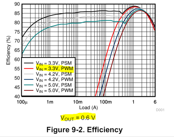
1). Comparing data sheet application curves from TPS62870-73 (10.2.3) vs. TPS62874-77 (9.2.3) there is an implication that the x71 for example is more efficient at our desired operating point. However, using a Webench based design comparison the x74 is more efficient as mentioned above. As a baseline i tried to determine the discrepancy between Webench and the data sheets. For a 3.3 VIN, 0.75 @ max device current a x73 design seems to match Fig 10-6 of the data sheet whereas the x77 design efficiency chart seems to be high by about 2-4 % (depending on current) from the Fig 9-5 x77 data sheet. Can you please verify my understanding and if there is a real discrepancy between Webench analysis and the data sheet? I am targeting the x74 for selection based on efficiency although the droop compensation feature might be of benefit as well.
2) The x74-77 family seems to share the same basic CMC architecture with the x70-73 family. However, some of the design formulas for component selection have differences between the "Typical Application". Can you confirm that the differences are intentional and that the Webench design is using these equations? One parameter of interest is what is Webench using for load step? Is it the maximum current? Also, for the x74 device there was a statement in 8.3.7.5 of its' data sheet implying the output capacitance can be reduced if droop compensation is enabled. Does the Webench based design take droop compensation into account?
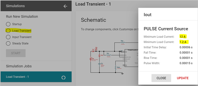
3) Input current measurement will be required for the given ASIC rail under test. Initially was hoping to use the inductor DCR current sense method but it appears that the combination of low DCR for the recommended inductors and also DCR tolerance will result in insufficient measurement accuracy. Proposing to add a discrete 10 mohm sense resistor in series with the inductor before the output capacitors. From the PSPICE simulation for the x74 device (average transient model) it appears that the only impact of the sense resistor is to extend the settling time after a load step by ~10 us. This should be ok for our application. I can envision the sense resistor addition won't be ideal from a layout perspective as it seems like the output capacitors might need to sit further away from the IC. Can you comment on any negative impact such as to layout or otherwise to consider?
Thank you very much for your time and consideration.