This thread has been locked.

If you have a related question, please click the "Ask a related question" button in the top right corner. The newly created question will be automatically linked to this question.

UCC21222: My UCC21222 drivers don't prevent simultaneous shoot through at the outputs. What can be wrong?

Part Number: UCC21222


Tool/software:

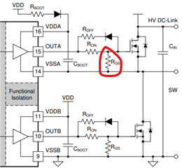
Each UCC21222D chip drives the half-bridge consisting of P-channel (high side) and N-channel (low side) MOSFETs. Unfortunately due to a problem in the logic, sometimes we get simultaneous positive pulses on both inputs. We are working to find and fix this problem but meantime for awhile our last hope for the prevention of a shoot through  is this feature of the chip to prevent simultaneous outputs and also a dead time setup. Dead time set to ~ 1uS by 100kOhm resistor. We have both output channels powered by the same 12V source bypassed by two caps 0.1uF and 4.7uF . There is chance that there is a short glitch - drop in this 12V output driving source but so far oscilloscope has not caught such drop.

Yet, MOSFETs are getting burned when input active pulses arrive simultaneously.  What could be wrong? Why the chip does not prevent simultaneous outputs? Is there errata on this driver chip ?

Please help.

  • Hi Vlad,

    Thank you for reaching out on E2E.

    If you have any waveforms captured at the time of failure and also during normal operating, those would be helpful to see if there is anything unusual.

    Waveform captures of the input side supply, output side supply, input, and output waveforms would be a good first step to see if there is unusual noise.

    One common cause of accidental MOSFET turn-ons is due to miller current.

    A gate to source pull-down resistor can be placed to help mitigate the risk of dV/dt induced turn-on due to miller current. A value of about 5.1kohm-20kohm should be sufficient.

    Regards,

    Hiroki

  • Dear Hiroki-san, thank you for your reply that implies that the problem could only be caused by the external components. Dropping the driver chip from the possible culprits reduces the work of debugging. 

    Unfortunately to take more screenshots from the oscilloscope and logic analyzer will take time as I need to restore lots of burned components before firing again.

    Please take a look at my half-bridge schematic based on the UCC21222D driver. This, in turn, based on the TI app note https://www.ti.com/lit/ml/slua618a/slua618a.pdf?ts=1688589306553

    example fig. 21 . My schematic worked well before I started testing a new motor which has significantly increased current and inductance in the coils.

    Now I became suspicious about two capacitors: C5 and C6.

    C6 slows down charging the gate of Nmos through R8 and C6 delay. The discharge is 10x quicker through R9-C6... I might need to drop R9 altogether to make a discharge of the gate to shut down Nmos immediately without a delay.

    I am more concerned regarding C5 cap ... TI' app note example does not have this cap. I don't remember exactly how it came about but I know it was introduced in the Spice simulation probably to slow down negatively charging the gate of Q3 to delay it's opening. This was observed in the Spice simulation.

    Now I am not sure with C5 role when drop of the main source happens during the motor coils energizing. This drop is significant. If Q3 was closed, C5 discharged, potential difference between Pmos S-G is 0. When short time drop of the main+ voltage source occurs I am not sure what happens Confused Is it possible that for a short duration of the negative spike on the main+ source the Pmos gate will be positive in relation to the Source? This is not allowed in P-MOSFETS...

    Some more details: in that schematic Q1 plays role of a level shifter and inverter, Q2 accelerates the charge and discharge of the Q3 gate. As you can see all the Nmos gates have been pulled down to the ground via 10K resistors.

    Please share your thoughts.

    Thanks in advance,

    Vlad

  • Hi Vlad,

    Thank you for providing all of these helpful details!

    A lot of good points made here.

    For the C6 capacitor, would it be necessary to have an additional gate to source capacitor with the high gate resistance? Was this added to intentionally slow down the switching or dampen the transients?

    For clarification, OUTA is driving a MAIN+ which is connected to a PMOS?

    Regards,

    Hiroki

  • This is a half bridge, the A OUT is a point connected to the one end of the motor coils, whence depending on which MOSFET is opened , the current flows either from the MAIN+ to the A OUT coils (if Q3 is opened) or, if Q4 is opened, flows from A OUT to the ground. C6 was meant to slow down positive charge of Q4 gate via R8-C6 low pass filter driven from the output of UCC21222 driver. Discharge is minimally slowed through R9-C6 low pass filter (probably R9 could be dropped).

    I have more concern about C5 at the time when Q3 is closed (Gate voltage equals Main+) yet a spike drop occurs in Main+ voltage supply... I can't understand the flow of current in this scenario...although it is clear the C5 role during the build-up of Main+ (it is shown in simulation as slowing the rising edge of the gate voltage)

  • Actually D1 Transient Volt Suppressor diode suppose to cancel any negative spike to the Pmos gate. Whence the C5 only works at slowing down the rise of Main+ Source which is it's intended purpose.

    I can't find any problem here. Yet MOSFETS keep burning when wrong input pulses activate both A and B channels... Disappointed  May be this has to do with Back-EMF from the motor coil when Q3 is closed?...

  • Hi Vlad,

    The C5 capacitor introduces add a significant amount of Miller capacitance to the high-side FET. 

    I am thinking this increased Miller capacitance is allowing more Miller current (i = C*dV/dt) to flow into the gate of Q3, which is usually the cause of dV/dt induced accidental turn-on of a MOSFET.

    Refer to 3.5 dV/dt Protection of Laszlo's Fundamentals of MOSFET and IGBT Gate Driver Circuits.

    Decreasing C5 and adding a sufficiently sized pull down resistor to prevent dV/dt turn-ons are ways to help prevent this from occurring.

    Hope this is helps with the issue.

    Regards,

    Hiroki

  • Hi Hiroki-san, yours seems to be valuable information in the right direction. I am trying to understand the following though : the Ch. 3.5 from the Laszlo'f Fundamentals (formulas 20 through 23) takes into account only Cgd gate-to-drain capacitance (I don't understand why), he does not mention Cgs capacitance, whereas we have C5 which is gate-to-source capacitance. If a total gate capacitance should effect the Miller effect (slowing down ON-OFF switching of MOSFET), then why Cgs capacitance is not mentioned in this chapter topic ?

    If we find out that C5 is to be reduced then, I guess, C6 must be reduced accordingly (or even both removed?)...because both C5 and C6 must match timing of ON-OFF switching of High and Low sides.  Is it so?

    Thank you for this valuable input, waiting for your reply,

    Sincerely,

    Vlad

  • Hi Vlad,

    Sorry I misinterpreted the Q3 MOSFET as an NMOS in my recent reply. In this case, reducing C5 would increase the switching times which could increase the dV/dt.

    To answer your question, the gate to drain capacitance is the primary focus in dV/dt induced turn-ons because of its dominant capacitance due to the Miller effect. 

    I would recommend trying a pull-up resistor at the gate of Q3 to prevent dV/dt induced turn-on on the PMOS. The calculations for the pull-up resistor sizing would follow Laszlo's application note.

    Please let me know if this works!

    Regards,

    Hiroki

  • In Spice simulation trying a pull-up resistor for the gate of Q3 did not change anything... still huge spike current at the opening  of Q3 Pmos... even a pullup value as low as 1K did not help... I think this is because the Q2 complementary BJP transistors bypass the pullup resistor with their lower resistance, after all this is their purpose to accelerate the charge/discharge of the Pmos gate. Laszlo did not include pullup when using Pmos Fig. 20 ...

    I know something is wrong here but it is tough task...

    I appreciate your help Hiroki,

    Vlad

  • Hi Vlad,

    Thank you for following up with simulation results! You make great points here.

    Looks like with the level shifted bipolar totempole circuit, reducing the pull up resistor (R4 in your schematic) increases the dV/dt immunity. Seeing as how increasing the current in the motor coils by switching to a new motor coil caused this issue, this points towards dV/dt turn-on.

    However to consider other possibilities, monitoring the gate to source voltages of the high-side and low-side MOSFETs will be good to ensure that the turn-on and turn-off timings at the load is sufficient and not causing any overlap.

    To help better understand the operation at the load, could you clarify how MAIN+ and Bridge A OUT is connected? Is the motor coil between MAIN+ and Bridge A OUT?

    Regards,

    Hiroki

  • Hi Hiroki, the full bridge consists of two half-bridges of the same schematic. The output of the half-bridge (bridge A OUT) shown in earlier linked schematic connects to the other half-bridge output (bridge B OUT) of similar schematic whence not shown there as they are the same.

    Both half-bridges share the same Main+ and GND power rails.

    Hope this explains the intend and workings of this half-bridge.

    Sincerely

    Vlad

  • Thank you for the explanation!

    Please let me know if my suggestions above helped at all.

    Regards,

    Hiroki

  • Hiroki-san, please confirm my understanding that all your suggestions imply that the problem could be only in the external schematic components while the UCC21222 chip definitely prevents from the shoot-through in the event of simultaneous triggering inputs, meaning the driver chip outputs never trigger both high and low Pmos gates simultaneously no matter what. Is it so?

    If this is the case, my problem research narrows and I got the initial help here.

    Sincerely

    Vlad

  • Hi Vlad,

    Yes, with the deadtime configuration enabled, the gate driver itself would not allow both outputs to be simultaneously on. 

    With higher current in the load causing this issue, it points towards external factors such as dV/dt induced turn-on. 

    Closing thread for now but please feel free to ask questions below if run into any further issues. I will be happy to provide my inputs.

    Regards,

    Hiroki