This thread has been locked.

If you have a related question, please click the "Ask a related question" button in the top right corner. The newly created question will be automatically linked to this question.

UCC21550: UCC21550 upper MOSFET driving circuit is not working

Part Number: UCC21550


Tool/software:

Hi,

I've used UCC21550ADWR  half bridge isolated gate driver IC to drive the MOSFET. Here I'm facing some issue while driving. . Below are the attached schematic which I'm using to drive the half bridge MOSFET. 

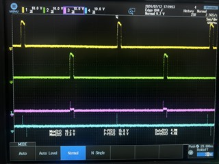
Issue : I'm using 3525 IC for PWM generation and during ON time both PWM is ON from 3525 IC  (Waveform attached) but in driver UCC21550 side, only Lower pulse is ON but upper pulse is off. 

Kindly check the schematic, Let me know if any changes required in components value.

Testing conditions:

1. Check with system (connecting both driver signals (OUT A & OUT B same as VSSA & VSSB  to MOSFET)

2. Changed the values of DIS and DT pins - No result

Your early response is valuable for me.

Thanks.


  • Hi Ravi,

    Firstly, I'd like to verify that your INA and INB voltage values are within the recommended operating conditions of the part. Based on your waveforms, they appear to be at around 12-15V, and our recommended range for INx goes up to roughly 6V. My recommendation is to keep the high pulse voltages around your VCC value to ensure a better lifetime of the part.

    Now in terms of your OUTA channel not switching, your schematic appears to be fine. The component selection aligns with all of our recommendations. I am curious where you are probing for the OUTA waveform. Are you probing at the OUTA pin, or are you probing closer to the mosfet? Same thing goes for the input waveforms. Are they also being probed at the pin, or further away? I want to be certain that the gate driver is in fact receiving the input signal, in order to better determine the root cause of the problem.

    Best regards,

    Will

  • Hi, 

    Thanks for the information. As I already mentioned in the attached schematic input supply voltage VCC= 5V. Also, INA & INB measured directly in 3525 IC (PWM generate) and OUTA and OUT B probes are connected at MOSFET side. 

    If there any calculation sheet available for this, please share with me.

    Kindly update if you need any other information. Looking your further guidance.

    Thanks.

  • Hi Ravi,

    Thanks for the additional information. Can you confirm for me that the voltage for VDDA and VDDB directly at the pin are both 15V? If you have waveforms probed at the pins VDDA and VDDB, that would help greatly. I want to be certain that channel A is receiving the proper voltage at the VDDA pin so that the device does not enter UVLO.

    Best regards,

    Will

  • Due to some changes in connection, now both the PWM are okay (Waveform 1 attached) (Testing condition: When Upper MOSFET Drain is open).

    But when I'm connecting the upper MOSFET drain, both MOSFET (upper and lower of Half bridge) are burned (waveform 2 & 3 attached).


    Need your suggestion, if I need to change any components value in the driver circuit.

    Thanks.

  • Hi Ravi,

    I'm glad you were able to figure out the issue regarding OUTA not switching. Now for the MOSFET outputs, either two things could be causing this behavior: 1) something may be affecting your input PWM pulses, as they look much different than the initial screenshot you sent first. 2) if the PWM inputs are behaving as intended, first ensure that you are not exceeding any voltage or current limitations for your MOSFET, and also ensure that you are not operating in the MOSFET's linear region since the increased drain-source resistance can lead to thermal damage. Our different UVLO options help to prevent this issue in most cases, so make sure you are utilizing the right UVLO option for your MOSFET specifications.

    Best regards,

    Will

  • MOSFET is burned in during gate driving (first gate pulse). Kindly verify the below schematic and waveform. Anything I need to change in schematic components please suggest. Also verify the gate driving components.

    Here PWM IC 3525 Voltage level is 12V. So I've connected voltage divider.


    MOSFET burned conditions:  


  • Hi Ravi,

    After looking at your waveforms (assuming yellow is OUTA and green is OUTB), it appears that OUTB may be turning on while OUTA is still high, potentially resulting in shoot-through. Please confirm that your PWM inputs as well as dead time configuration is sufficient enough to allow the OUTA channel to be turned off before OUTB is turned on.

    Best regards,

    Will

  • Hi,

    PWM input voltage is 12V. I've connected divider at INA and INB side  to convert the same in 5V .

    Below are the waveform when I am changing supply side capacitor i.e. 

    VDDA = 100uF Ele. &  100nF ceramic


    VDDB  = 10uF ELE & 100 nF ceramic.


    Please share if any calculation sheet is available. How I can verify the Dead time. Please suggest.

  • After some changes in circuit now system is working but, some noise is receiving at INA and INB signals while Both MOSFET are conduct.  

    Blue and Pink signals are - INA and INB

    Yellow- Upper VGS

    Green- Lower VGS

  • Hi Ravi,

    Dead time can be calculated with the following equation:

    t (in ns) = 8.6 * RDT (in kΩ) + 13

    the resulting dead time will have a tolerance of +/- 10%.

    At the moment it is difficult to tell the source of the noise. Do you have any more information regarding the noise shown in those waveforms, and how they correlate with your input signals?

    Best regards,

    Will