This thread has been locked.

If you have a related question, please click the "Ask a related question" button in the top right corner. The newly created question will be automatically linked to this question.

LM25180-Q1: Schematic Review & Question

Part Number: LM25180-Q1

Tool/software:

Hi TI team,

My customer made the board and started the functional test.

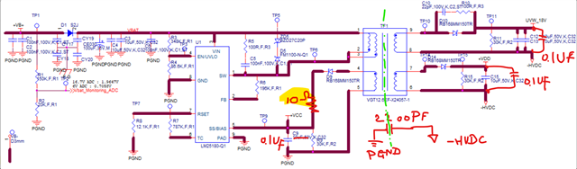
But the board doesn't work, so please review the schematic.

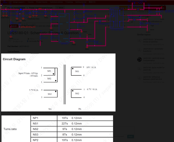
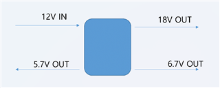
The auxiliary winding is designed to output 5.7V from the primary side.

Q1. Please guide the data on the Transformer Auxiliary Winding of 5 pins.

  • Hi 

    Thank you for posting.  Sorry I cannot read the schematic because when I click to open it, it shows in dark color (see the snapshot on my computer display). Could you resend a legible schematic, and also tell me their transformer's Lmag and Isat?  

    Thanks,

    Youhao

  • Hi Youhao,

    Schematic update.

    There is no Isat information in the customer's data.

    Lmag : 41.5Uh

  • Thank you for the info.  I reviewed the schematic it basically looks okay. Here are some comments for the customer to consider:

    • I would reduce the VBIAS capacitor to 1uF max (try 0.1uF at the beginning), because the capacitor also affects the start up time.  I would also insert a 5 to 10 Ohm resistor in series with the resistor to prevent excessive voltage (and to save a Zener clamp there).
    • I would reserve the positions of the other three small capacitors in case they are needed after test.  It is a good practice to have 0.1uF at each out rail to filter out high frequency switching noises.  It is also good to have a Y-cap across the isolation boundary (dashed green line) to confine noise within the circuit and prevent it from emission.   These capacitors can be place holders on your PCB and you can decide use or not use them after tests.

    Please refer to the datasheet layout guidelines, and also to our EVM layout examples when designing your PCB.

    Hope this helps.

    Regards,

    Youhao

  • Hi Youhao,

    Thank you for your support.

    It doesn't work even if it reflects what you explained.

    Q1. Please guide the data on the Transformer Auxiliary Winding of 5 pins.

    Additional explanation.

    D: Short key diode (not Zener)

    When the R3/R4 resistance is removed, no switching is performed.

    When R3/R4 resistance is applied, it is 6V output.

    The switching frequency is only a few tens of keys.

    Flyback Flowchart :

    5.7V is the output of the primary side auxiliary winding.

  • This is the result of the customer's review.

    Removing D9, D14 of the transformer produces 20V output from UVW_18V.

    Is it correct to connect 5.7V of Transformer pin 4 to SS/BIAS?

    Is it not output due to the winding ratio of the transformer?

    If there is no problem with the winding ratio, please guide me if there is any way to improve it in the schematic.

  • Hi CHO,

    Can you ask the customer to share the complete transformer datasheet?  SS/BIAS can be supplied from a transformer winding but they  may need to reduce that cap and also insert a resistor as I mentioned in the schematic markup.

    Also, please note that there is a min load requirement.  I am not sure if the 30k across the output rails are adequate to meet the min load requirement.  Please help get the transformer datasheet.

    The typical min load = 0.5 * Lmag * 0.3A^2 * 12kHz 

    Therefore, they should not test the circuit without load.

    Regards,

    Youhao