


TI gate drivers use a pull-up and pull-down structure in the output stage in order to drive a power device. The pull-up structure supplies the source current to turn on the power device, and the pull-down structure supplies the sink current to turn off the power device. Traditional gate drivers supply the source and sink currents through a single output pin; however, some gate drivers feature split outputs, which have separate pins for sourcing and sinking currents. Source current takes the “turn-on” path and sink current takes the “turn-off path”. Figure 1 shows the output stage of a gate driver with a single output, while figure 2 shows the output stage of a gate driver with split outputs.
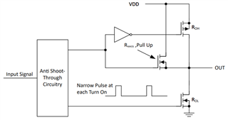
Figure 1: Gate driver output stage with single output
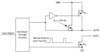
Figure 2: Gate driver output stage with split outputs
For power devices, rise time, fall time, and turn-on and turn-off delays are typically different. Gate resistances are used to control these characteristics. A lower gate resistance on the turn-off path allows for a faster turn-off and can also help prevent false turn-on caused by fast switching and Miller current. Likewise, a lower gate resistance on the turn-on path can result in faster turn-on, which reduces switching losses. Careful consideration of the system design and behavior is needed when adjusting the gate resistances.
A gate driver with a single output can use a diode in parallel with the gate resistor to adjust the turn-on and turn-off path separately. Figure 3 shows the orientation of the diode D1 for faster turn-off. When the gate driver sources current, the diode blocks the current flow in the path with no resistance. This causes the source current to go through resistor R1 only, making the turn-on gate resistance 2.2Ω. When the gate driver sinks current, the diode permits the current flow and ideally reduces the turn-off gate resistance to 1.1Ω. A resistor can be placed in series with the diode to adjust the turn-off path as needed. For a faster turn-on, simply reverse the diode orientation.
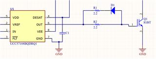
Figure 3: Using a diode for a faster turn-off in a gate driver with single output
A gate driver with split outputs gives the benefit of separately controlling the turn-on and turn-off path without a diode. This advantage shines brighter with gate drivers that have different source and sink current strengths (e.g. LMG1020, which has 7A source and 5A sink). The removal of diode saves PCB space for better layout and eliminates parasitics that come with the diode, both of which are important in fast switching applications such as GaN. Parasitic inductance that comes with the diode can lead to false pulses when the gate driver sinks current rapidly (V = L * di/dt). These false pulses can be small, but large enough such that it reaches the turn-on threshold of the FET. Repeated pulses that barely turn on the FET can damage the FET overtime due to conduction losses. The diode will also increase the bill of materials cost. Figure 4 shows how a gate driver with split outputs can be used to achieve a faster turn-off compared to turn-on without the need for a diode.
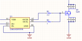
Figure 4: Using a gate driver with split outputs
Choosing between a gate driver with split output vs. single output boils down to the project requirements and layout concerns. In many cases, a gate driver opting for a split output feature means that another feature is replaced. For example, the UCC57108C variant has split outputs, but it replaces the VEE feature found in the UCC57108B variant. If using a single-output gate driver is unavoidable, then it is recommended to select a Schottky diode with low forward voltage, fast response time, and small parasitics.
