Other Parts Discussed in Thread: LM74930-Q1
Tool/software:
Hey there,
If I may, a bit of a sanity check that I am not about to do anything outside the scope of the device, and a couple of questions.
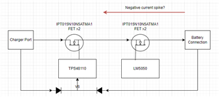
I have an application where I need to dynamically connect a charger (up to 90A) to a battery system (48V), and have OV, UV and over current protection. It also needs to ensure that no voltage is present at the charging port from the batteries in the situation where the TPS is told to turn 'off' (INP low). The charger will not provide power unless it sees a (battery) voltage at the charger port, so I need to power the TPS48110 via diode oring as per the EVM schematic. I think my general scheme for this (shown below) is ok.
1. I have a concern that if the charger is disconnected under load, there might be a negative going current spike from the battery end due to the inductance in the cables. The cables are short, but naturally I don't want to blow anything up and I presume this spike could destroy the mosfets. In order to prevent this, I was looking at reverse current protection (battery back out towards charger) but am a bit confused by two options.
I see on this answer (https://e2e.ti.com/support/power-management-group/power-management/f/power-management-forum/1343268/tps4811-q1-working-with-motors-back-emf-problems/5122464?tisearch=e2e-sitesearch&keymatch=TPS4811%252520lm5050#5122464) you have suggested an LM5050 to prevent such a spike due to back EMF, but was wondering whether the back-to-back mosfet set up shown in the TPS datasheet (page 25) will also do reverse current protection (similar to how the LM74930-Q1 seems to)?
2. I am unsure what factors are involved in determining the maximum number of mosfets the TPS and LM5050 can drive. I currently have two (option for a third for thermal considerations) IPT015N10N5ATMA1 mosfets being driven by each of the chips. I have read that the TPS can drive multiple fets and the LM5050 can drive at least two. Any guidance on how I determine the maximum drive ability of them would be helpful.
Thanks again!