This thread has been locked.

If you have a related question, please click the "Ask a related question" button in the top right corner. The newly created question will be automatically linked to this question.

LM3691: Absolute maximum rating

Part Number: LM3691

Tool/software:

Hi Team,

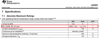
Customer is asking the absolute maximum rating for switching node.

They assume the absolute spec is only DC rating, The AC (less than 10ns) Absolute Maximum Ratings for the SW pin (while switching) would be: min = -3.0V, max = 9V.

Per my understanding, -3V will cause low side switch body diode conduction and high current flow; 9V will cause high side switch body diode conduction and high current flow, which will possibly damage the device.

Could you please help to comment on the AC (less than 10ns) Absolute Maximum Ratings? Thanks.

Regards,

Terry

  • Hi Terry,

    The SW ratings in the datasheet is DC. You can take around -3V to 9V for 10ns for the AC ratings.

    The negative AC spike is because of the conduction through the low side FET body diode as you said. The positive AC spike, this is mostly due to the parasitic inductance between the input cap and the high side FET. When the high side FET is turned on, there is a high current spike from input to supply the reverse recovery charge of the low side FET and then charge the low side FET capacitance. Since this current is only a transient current, the parasitic input inductance causes an overshoot when this current subsides. Adding the input cap close to the VIN and GND pins of the IC is helpful to reduce this parasitic inductance and overshoots on the SW node.

    Best regards,

    Varun