Other Parts Discussed in Thread: LMR54410
Tool/software:
Dear TI support,
We have a number of battery-operated devices w/ LMR14010A regulators that have been running in the field for the past year or so, and we recently discovered that the batteries are not lasting as long as expected. We brought some of the devices into the lab to investigate, and found that LMR14010A power consumption is the culprit, and that swapping out the LMR14010A for a fresh one (while leaving all of the same passive components in place) brings the devices back into compliance.
Setup notes
--Vin ~= 14.4 V, from a battery pack
--Vout = 3.3 V
--I_load is typically 1-2mA (99.9% of the time)
--I_load_max is < 50mA (the other 0.1% of the time)
--Our devices are always on, so LMR14010 runs continuously
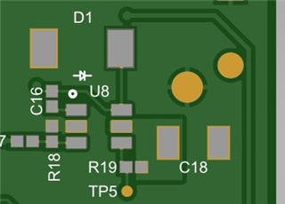
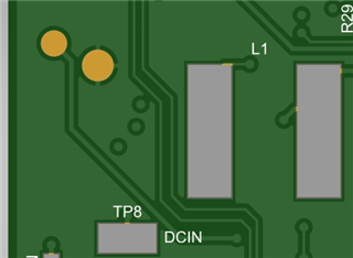
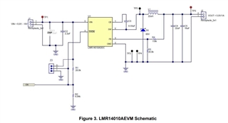
--Schematic:

Observations
When devices are pulled from the field:
-I_quiescent (LMR14010A load disconnected) = 800-1000 uA
-Vout_no_load = 3.40 - 3.45 V -- which is outside the tolerance of the 1% feedback resistors
-Vfb is usually higher than spec, e.g. 0.850 V
After replacing just the LMR14010A (all of the passive components are left in place):
-I_quiescent =~ 50-70 uA
-Vout = 3.31 - 3.33 V -- which is within the tolerance of the 1% feedback resistors
-Vfb is within spec
This same behavior has been observed on multiple (~half dozen) devices tested so far.
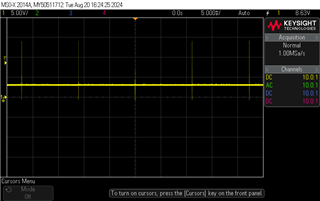
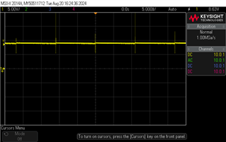
We're also running two side-by-side LMR14010A EVMs -- one with an old LMR14010A pulled off one of our devices, and the other with a fresh LMR14010A. All of the dev board components are stock, except for the feedback resistors (64.9k, 19.6k) to set Vout = 3.3V, and the inductor (120uH).
EVM observations
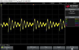
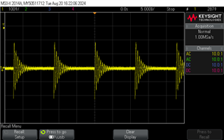
Old LMR14010A:
No load:
I_quiescent = 911 uA
With 50mA load applied:
P_in = V_in * I_in = 14.37 V * 23.62 mA = 339.4 mW
P_out = V_out * I_out = 3.42V * 50mA = 171.0 mW
Efficiency = 171.0 / 339.4 = 50.4% --> very low efficiency
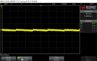
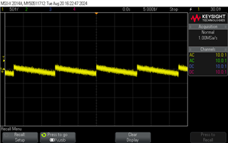
New LMR14010A:
No load:
I_quiescent = 68 uA
With 50mA load applied:
P_in = V_in * I_in = 14.38 V * 14.08 mA = 202.5 mW
P_out = V_out * I_out = 3.28 V * 50 mA = 164 mW
Efficiency = 164 / 202.5 = 81.0% --> consistent with Fig. 5-2 in the LMR14010A datasheet
Any thoughts on what may be causing the high power consumption / low efficiency in older devices? Thank you.