This thread has been locked.

If you have a related question, please click the "Ask a related question" button in the top right corner. The newly created question will be automatically linked to this question.

TPS22811: Question about floating input

Part Number: TPS22811

Tool/software:

Dear TI experts,

My customer considers TPS22811 for specific purpose.

They chek the step as follows, based on block diaram of TPS22811.

1. Apply 12V to output, and leave input floating.

2. FFT signal is activated due to voltage drop of body diode of HFET.

3. PG pin is reset.

4. Using this PG low signal to control other IC. (EN pin low)

(They added 200~400ohm resistor between input pin and GND to make large voltage drop of body diode of HFET, make 30~60mA current as a result.)

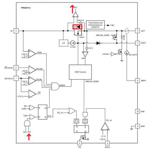
At first they checked that  voltage difference between input and output pin is enough, so PG pin is pulled to low as they expected.

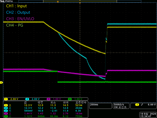
But some time passed, waveform changed a little as below and PG pin is not pulled to low.

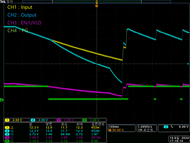
They expect that body diode of HFET is broken so the voltage difference is not made to PG pin low.

- Here are my questions ;

1. I want to confirm that the sequences of my customer (1. to 4.) make sense or not.

2. Is it right to use FFT signal to control PG pin?

I can find onlt the relationship between PG in and PGTH, but nothing else.

3. They need to use strong pullup for PG pin to control external IC. (need to make 5mA or higher current)

But datasheet says that strong pullup yields just 242uA current. Can my customer us stronger pullup?

Please check these issues. Thanks.

Best regards,

Chase

  • Hello Chase,

    From the waveforms I can see the VOUT is going low. You wrote you are applying 12V at output.

    Can you share the schematic?

    Need to check how EN pin is connected since EN coming up again.

    Device is showing expected behavior from waveforms. 

    EN going low making the PG down and again after some time EN pin coming back making PG high.

    Thanks 

    Amrit 

  • Dear Amrit,

    Thank you for your support.

    I will ask about the waveform, and send you the updates.

    - Do you think that it is make sense of the situation above of floating input and 12V applied output?

    - What do you think about the reason of not making PG pin low? Does it have any possibility of HFET broken?

    Best regards,

    Chase

  • Hello Chase,

    PG is going low because of EN/UVLO going low. Which is causing the circuit to go into protection.

    Please clarify the exact test procedure customer is performing. I can see VOUT is drooping but you said they are applying fixed 12V VOUT. 

    Thanks

    Amrit 

  • Dear Amrit,

    Thank you for your support.

    First i attach the simplified schematic and block diagram.

    - The device can use one of 2 sources, 12V from PoE or 12V adapter.

    - 12V from PoE is supplied by TPS23754->Active forward converter.

    - 12V adapter is supplied by external adapter. its routing is connected to the output of TPS22811.

    (the input of TPS22811 is connected to 12V PoE from Active forward block.)

    - They want the priority of power to 12V adapter even 12V from PoE is applied.

    - So they thought about the schematic how they can give the priority to 12V adapter, so they thought about the diagram above.

    - the situation of floating input and 12V output is assumed disconnected 12V PoE and applied 12V adapter.

    - And the first waveforms above is about the situation of applying 12V adapter while 12V PoE is applied.

    You can see PG pin is going to low, it is the moment of applying 12V adapter while 12V PoE is applied. And about 400ms time passed, final 12V is switched to 12V adapter successfully.

    But in the second waveform, I could find that PG pin is going low in the monemt of 12V adapter is applied. but PG pin is going to high again and making pulse signal. That is why I suspect about broken HFET.

    And here are my questions again ;

    1. Do you think that it is make sense of the situation above of floating input and 12V applied output?

    2. What do you think about the broken FET? Do you think that it is the reason of not making the waveforms as they expected?

    Please check these issues. Thanks.

    Best regards,

    Chase

  • Hello Chase,

    Thanks a lot for the detailed explanation.

    I will get on this after analyzing.

    Thanks\

    Amrit  

  • Dear Amrit,

    Thank you for your support, and hope you have a good day.

    Please let me know if there are any updates about the issue above.

    Best regards,

    Chase

  • Hi Chase,

    I will be taking over this question.

    I have a quick question. What is the system use case for connecting 12V adapter at Vout and POE 12V at the input. Do they want a priority powerMUX here? 

    Where are they connecting there load?

    Best Regards,
    Arush

  • Dear Arush,

     Thank you for your support.

    1-1. They assume that applying 12V adapter power while they use 48V POE->12V voltage already.

    1-2. Yes. They want to give priority to 12V adapter power.

    2. The load is connected to "MAIN SYSTEM", the green box of block diagram above.

    Please let me know if you need more information.

    Best regards,

    Chase

  • Hi Chase,

    Can we have a quick meeting regarding this. I think I am little confused here. My understanding till now is they have connected POE converted to 12V at the input of load switch and 12V DC adaptor at output of load switch. Not sure where the main system is connected. 

    12V adapter is supplied by external adapter. its routing is connected to the output of TPS22811.

    (the input of TPS22811 is connected to 12V PoE from Active forward block.)

    I have sent you friend request. We can align on the meeting details over E2E DM. 

    Best Regards,
    Arush