This thread has been locked.

If you have a related question, please click the "Ask a related question" button in the top right corner. The newly created question will be automatically linked to this question.

TLV760: Schottky path consume backup charge

Part Number: TLV760

Tool/software:

Hi team,

Customer will use TLV76050 and wants to add large capacitor in output for MCU.

Once the input shut down, I recommended Schottky diode being parallels with LDO to prevent reverse current.

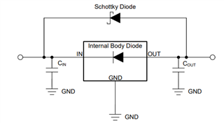
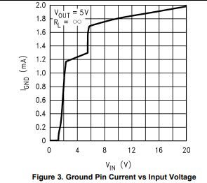
However, there is another concern that, does LDO consume current from Schottky to VIN like below?

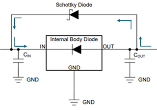
I think that VIN will be Hi-Z when no input voltage, so consumed current is not so much. However, how to calculate it?

Best regards,

Hayashi

  • Hey Hayashi,


    Generally, in this implementation, the assumption we take is that when input supply goes away, VIN is connected to ground and hence the output capacitor discharges to ground through Schottky diode. 

    But as you mentioned, if VIN node is in Hi-Z config, there is going to be a charge sharing mechanism between Cout and Cin. Due to which some kind of voltage can be developed on the VIN pin of the LDO as the current flow path that you mentioned can happen. 

    But as VIN is always lower than VOUT pin, Part will always be in dropout operation and there is going to be a current flow through LDO ground (quiescent current). 

    In the datasheet of TLV760 (Fig 3), IQ vs VIN is captured, where depending upon VIN level, the current flowing to ground can be roughly estimated. 

    Please review and let me know if further details are needed.


    Regards,
    Rohit Phogat

  • Hi Rohit,

    When input supply stops, the voltage on the IN pin gradually decreases, while the OUT side is kept at 5V with the backup of a 1F capacitor.
    If the current does not flow because of the high impedance between IN and GND, where is the current that flows to the input side through the Schottky diode consumed?

    Or is it because the IN-GND is high impedance, so the reverse current flow cannot occur with 5V backup as shown in the above figure?
    If not, is it necessary to consider a Schottky diode?

    Best regards,

    Hayashi

  • Hey Hayashi,

    Although IN-GND is a high impedance node, there is still going to be a potential on IN pin due to capacitive division between CIN & COUT.

    Could you please provide some information on the value of CIN/COUT in the customer's environment.


    Regards,
    Rohit 

  • Hi Rohit,

    Input cap and Output cap are both 0.1uF.

    regards,

    Hayashi

  • Hey Hayashi,

    I didn't realize that the thread is still open. If both CIN and COUT are equal the IN will charge to approx. 2.5V and in that situation the current through GND would be approx. 1.2mA (Fig 3). But if a large output capacitor is connected in that case, the IN will be at higher potential and can increase IGND consumption.

    Regards,
    Rohit