This thread has been locked.

If you have a related question, please click the "Ask a related question" button in the top right corner. The newly created question will be automatically linked to this question.

BQ76200: Odd behaviour on gate driver output

Part Number: BQ76200
Other Parts Discussed in Thread: BQ78350, , BQ76930

Tool/software:

Hello,

I am having an issue with the BQ76200 coupled with the BQ76930 and BQ78350.

The problem that I have is that the power MOSFETs are not fully turning on as it appears that there is a charge pump over load situation.

The schematic of the system is shown below for reference.

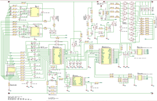
I have made obvious changes to the schematic of the BQ76200, changing the 0.1uF filter caps to 10nF and another board with 1nF caps.

Changed the VDDCP capacitance to 2.2uF and 4.4uF to cope with the amount of MOSFETs it is driving and placing 100 ohm resistors on the gates with no signs of improvement.

The BQ78350 is communicating fine with measured outputs on the CHG and DSG pins around 12.4V when powered by a 10S simulated cell board as shown below.

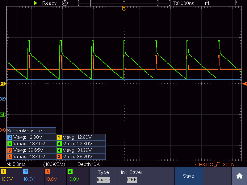
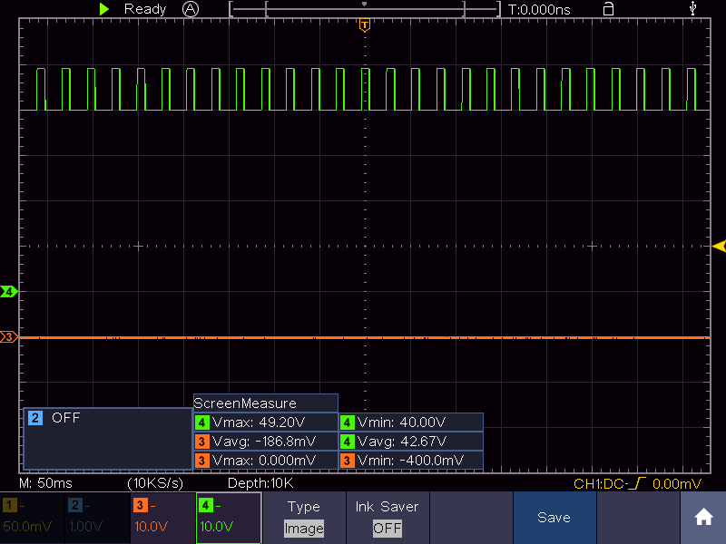
Scoped gate voltages can be seen in the image below.

CHG gate in green and DSG gate in orange, but this is only the case when both are active together.

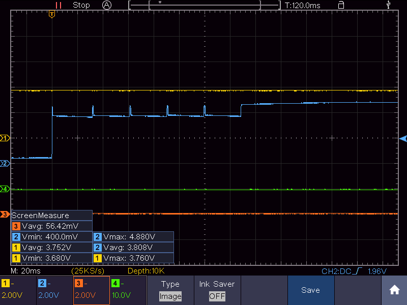
CHG output only was activated and scoped to show this square wave.

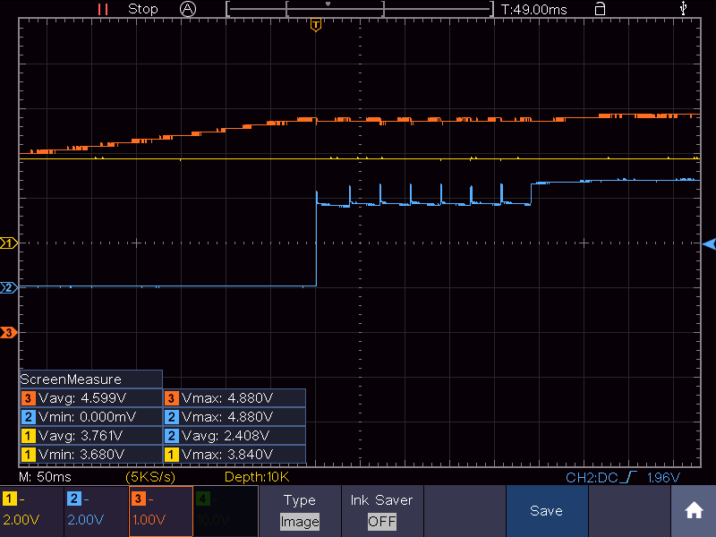
Again, CHG was deactivated and DSG was activated with the following result.

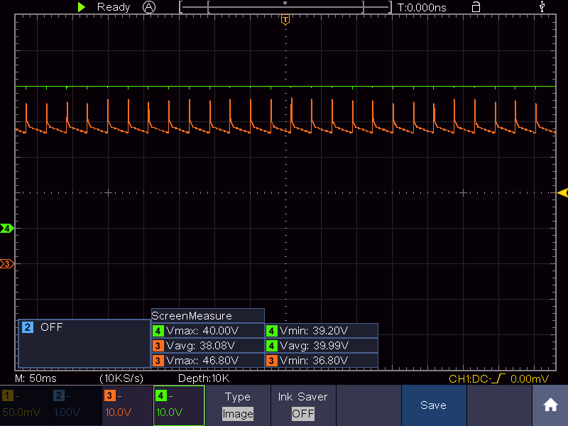
Interestingly the CHG output remained at pack level with some noise shown on the line which matches the peaks of the DSG output.

Any help in this matter would be greatly appreciated.

Many thanks,

Luke

  • Hello Luke,

    Yes the CHG pin actually connects to the BAT pin when it is OFF. 

    It does seem like the charge-pump may be getting overloaded (See bq76200 Beyond the Simple Application Schematic for reference). As a quick test, could you disconnect the CHG MOSFET from the pin and see if this still occurs?

    Could you also measure the CP1 pin to measure what is happening to its voltage? Also mind sharing a PDF/High-quality version of your schematic, it is somewhat hard to read from the image.

    Something else I notice is that there is no pin resistances for CHG/DSG, we usually recommend to have pin resistances of at least 100's of Ohms.

    Best Regards,

    Luis Hernandez Salomon

  • Thank you for your reply Luis.

    I've attached the schematic for your viewing.
    I tried to disconnect the CHG MOSFETs with no change to the DSG profile.

    Wasn't sure what you meant by CP1 pin?
    However, when active with a bat+ voltage of 40V, I am seeing 47.6V at the VDDCP pin and 0V at the CP_EN pin which is pulled to VSS as it is not in use.

    Would this cause an issue? I read in the datasheet that it should be logic gated internally using OR to the CHG and DSG EN pins.

    Many thanks,

    Luke

  • Hello Luke,

    Whoops I meant VDDCP pin! I mixed up names there haha.

    Would it be possible to get a waveform showing the DSG/CHG pins and CHG_EN/DSG_EN with the VDDCP pin voltage showing as well?

    Would this cause an issue? I read in the datasheet that it should be logic gated internally using OR to the CHG and DSG EN pins.

    Correct. This is OR'd, but if CP_EN is not set first, it will take some time for the charge-pump voltage to rise and enable the FETs.

    Best Regards,

    Luis Hernandez Salomon

  • Morning Luis,

    Ah good, I did interpret it correctly then haha

    Here is the shot of the inputs and outputs this morning.

    It's slightly different as I removed some ESD caps etc that might have been adding extra capacitance on the power input filters.
    I'm also down to 1 MOSFET on each side on this board to see if there was too much loading from having the 4 CHG, 8 DSG configuration.

    CH1 = CHG input from BQ76930 (12.8V, no noise)
    CH2 = DSG input from BQ76930 (12.8V, no noise)
    CH3 = DSG output from BQ76200
    CH4 = CHG output from BQ76200

    Many thanks,

    Luke

  • Hello Luke,

    Can you capture DSG/CHG output from BQ76200 with the VDDCP voltage?

    Now, this is still looking as if the charge-pump is getting overloaded for some reason. Is there high inrush currents to the FETs? What if the 10-MOhm resistors are removed? Is there any improvement?

    Maybe an ABA swap with an EVM could be good to check if it is an IC problem or board problem.

    From the schematic, I actually do not see how the charge-pump could be getting overloaded. So may be a good idea to check the board for leakages around the charge-pump or the CHG/DSG outputs.

    Best Regards,

    Luis Hernandez Salomon

  • Hello Luis,

    Small development since our last chat.

    The problem only appears to exist when both CHG and DSG FETs activate at the same time.

    If I activate the CHG FETs, wait less than a second and then activate the DSG FETs, the problem goes away and I can draw current as normal with full pack voltage being shown.

    If I probe the VDDCP pin with an oscilloscope then the output voltages collapse on the CHG and DSG pins.
    It could be placing too much load on the pins while measuring.

    At the moment, I am using a fresh board with 4.7uF VDDCP cap, 10nF filter caps and 2Kohm resistors to the FET gates (only thing I have to hand currently).

    Many thanks,

    Luke 

  • Hello Luke,

    What I am surprised that an oscilloscope would cause it to collapse, is it a 10x probe?

    Just from the sounds of this, it does sound like it is likely that the inrush current when turning both at the same time is causing the VDDCP voltage to drop low enough to turn-off the connection to the FET drivers. I am wondering why this is happening, and I find it strange that the oscilloscope would cause it to completely drop.

    You have 12.8-V battery, so assuming that VDDCP is ~11-V normally. Then VDDCP would be 23.8-V, a 10x probe may be 10-Meg, so ~2.4-uA or so. Not nearly enough to cause a collapse on the VDDCP voltage. 

    I feel like there may be leakage somewhere that could be causing this, or maybe a component with an erroneous value?

    Best Regards,

    Luis Hernandez Salomon

  • Morning Luis,

    I will investigate a bit more but from what I am seeing, the voltages are fine once the charge pump can be engaged long enough to activate them.

    CHG side appears fine with no odd behaviour, however, I have noticed that when switching the DSG FETs on then there is a notable tick and the IC struggles before full activation is achieved.

    Many thanks,

    Luke

  • Hey Luis,

    Sorry, I had the probes on x1 which was putting too much load on the pins.

    See below for charge pump pin timing in reference to switching DSG output on to the FETs.

    The voltage does not appear to be the issue as I am seeing roughly 11V above pack voltage.

    Many thanks,

    Luke

  • Hello Luke,

    I see, so the probes were part of the initial problem?

    From this image it does seem like the charge-pump does stabilize eventually and the MOSFETs are able to stay ON.

    It is likely from inrush currents as the MOSFET is beginning to turn-on.

    I think besides waiting for the driver to go to normal, the only other solution I can think of is for the charge-pump to be enabled a few hundred ms so that it stabilizes before turning the DSG/CHG FETs back ON.

    Best Regards,

    Luis Hernandez Salomon

  • Hi Luis,

    They were on the initial measuring.

    I'll need to check all the connections and go through all components step by step in order to see what is causing the drain on the charge pump.

    I will update this thread if I find anything but have placed 2K resistors on the charge MOSFETs and 4K resistors on the discharge FETs, removed the 10M resistors to pull the FETs to pack voltage, reduced the size of the smoothing capacitors and run a line from the BQ76930 2.5V regout to the CP_EN pin with some slight gains.

    There is still an audible noise when switching the DSG FETs so need to spend some time tracing current paths.

    Many thanks,

    Luke

  • Hello Luke, 

    Luis will get back to you tomorrow regarding this. Thank you for your patience.

    Best Regards,
    Alexis

  • Hello Luke,

    Understood! Do let us know what you find.

    By audible noise, do you mean that you can hear it? I am surprised that you would still see problems without the probes and even without the 10-Meg... 

    It definitely could be some leakage somewhere. But I am wondering, did try performing an ABA swap with a board like the EVM?

    Best Regards,

    Luis Hernandez Salomon