This thread has been locked.

If you have a related question, please click the "Ask a related question" button in the top right corner. The newly created question will be automatically linked to this question.

CSD23382F4: Dimension NG

Part Number: CSD23382F4

Tool/software:

Hi,

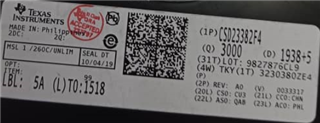
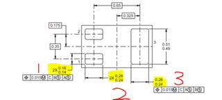
I’m writing here to bring the issue of dimension NG we are having now and seek for advice from Texas Instrument team. For your information, our team found dimension NG for three parts after measured with two samples. The machine we used to measure dimension is Pricis-VMG450 and its video measuring software, Measuremind. Through the software, we usually draw two lines and measure the gap between them to find the dimension. Please refer to the picture and table below for the details of measurement.


Part

Nominal (mm)

Tolerance

Dimension (mm)

Measured dimension (Sample 1) (mm)

Measured dimension (Sample 2) (mm)

LSL

USL

1

0.15

0.01

0.14

0.16

0.1588

0.1609 (NG)

2

0.25

0.01

0.24

0.26

0.2615 (NG)

0.2662 (NG)

3

0.25

0.01

0.24

0.26

0.2522

0.2627 (NG)


We hope to get support from Texas Instrument team and get advice on the questions below:

  1. Does these dimension NG consider as normal or abnormal?
  2. Would these dimension NG affecting the function of the component?
  3. Do we measure with the correct method? Please correct us if we are using the wrong method to measure dimension.


Thanks and best regards,

Cheah

  • Cheah,

    Thank you for contacting us, I will need to contact some packaging people and will get back to you as soon as possible.

    Many thanks

    Chris

  • Cheah,

    I have contacting our packaging experts and they have a few questions we would like for your to answer if possible, before we can answer your questions:

    1. These features are done at a wafer level so it is unlikely to have different values within the same wafer, in other words all units would fail or pass, unlike the measurements you have given in your table
      1. Could you please provide the lot number or TI lot trace code for the devices you have shown in your table, are they all one lot or different lots? We can then go and check our specific internal data to see if there was an issue.
    2. The way you describe the measurement seems to be user dependent and not automated.
      1. If manual was the measurement done only once?
      2. Can you repeat the measurement to see the repeatability of the measurements?
    3. We are unable to define the equipment you should use for your own process but can you double check on the calibration and make sure the software and equipment are up to date.
      1. The reason we say this is the equipment you mention, according to the specification, has a resolution of 0.001mm but your numbers report 0.0001mm
      2. We do not know if you have an enhanced version of this equipment capable of 10x better resolution than they specify for the std VMG-450 model.

    Many thanks

  • Hi Chris, 

    Sorry for late reply.

    1. The lot number for this device is 9827876CL9. They all are in one lot. 

    2. We have done the measurement three times. Each measured value is almost the same.

    3. The equipment and software that we used are calibrated and up to date. Actually, all the values measured are in 6 decimals number in unit of mm. I think it may because of the software we used able to support the measurement to 6 decimals number.

  • Hi Cheah,

    Chris is out of office today. Thanks for the updated information. Is this dimensional issue causing a problem with assembly of the devices onto the customer's board? We will review and get back to you when Chris returns next week.

    Thanks,

    John Wallace

    TI FET Applications

  • Hi John,

    We have not implement this device onto the board yet as this issue was found during our incoming inspection. The overall size of the device is within the spec however the dimension of footprint is larger than the spec in datasheet. Therefore, we afraid that this dimension NG of footprint would affecting the function of this device if we assembly the devices onto the board, and so I am writing here to seek for advice from Texas Instruments professional technicians. 

    Thank you.

    Best regards,

    Cheah 

  • Cheah,

    I am sorry but we were unable to find this 9827876CL9 in the system, do you have a photo of the shipping label on the box that you could send so we can go and check our manufacturing details. Or any other information you could please provide for this lot.

    Thanks

    Chris...

  • Hi Chris,

    This is the label for this lot.


    Many thanks,

    Cheah

  • Cheah,

    Thank you, we will investigate and be back to you ASAP

    Chris

  • Hi Cheah,

    Apologies for the delay. We are still waiting on more information from the factory and will update you as soon as we have it.

    Thanks,

    John

  • Hi Chris and John,

    Any update from the factory?

    Thanks,

    Cheah

  • Hi Cheah,

    We're still working to get the data. If the customer follows the recommendations for PCB layout and stencil design, they should have no problems placing and soldering these devices onto their PCB. The dimensional variation should not cause any reliability issues. Below is a link to the FemtoFET SMT guidelines. TI has shipped high volumes of these devices and there have been no reported issues due to the dimensional variation of the package. We will update you as soon as we have data to share.

    https://www.ti.com/lit/pdf/slra003

    Thanks,

    John

  • Hi Chris and John,

    It has already been passed 2 weeks. Do you have the data to update and share to us?

    Thanks,

    Cheah

  • Hi Cheah,

    Again, I apologize for how long this is taking to resolve. There is no measurement of pad sizes made on the individual FET die. The solderable pad dimensions are controlled by the tolerance in the fab which is around 0.25μm. TI finds it unlikely that these pad are out of specification and there might be a measurement issue. As I stated previously, you should have no problems assembling these parts onto the PCB if the PCB pad layout and stencil openings recommended in the datasheet and the FemtoFET SMT guidelines are followed. If you wish to pursue this further, then you can go thru the standard quality return process and contact your local TI quality and/or use the link below. Please let us know if you have any additional questions.

    https://www.ti.com/support-quality/additional-information/customer-returns.html

    Thanks,

    John