Tool/software:
Hello!
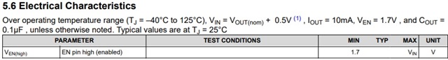
I am testing the TPS736 in a design, where I am supplying 3.3V to the VIN pin in order to generate a 1.8V output rail. I notice in the datasheet that VEN is typically between 1.7V and VIN for enabling the LDO, but I am driving the VEN pin with 5V and seeing nominal behavior, and am not seeing the VEN signal get shunted or clipped down at all. Since the IC is compliant to CMOS logic levels, is it acceptable to have VEN be at a higher voltage than VIN, so long as it is still within maximum operating conditions? Is there any damage done to the chip if VEN is 5V while VIN is 3.3V? Or is the lifetime reduced by this sort of setup?
Thanks