Tool/software:
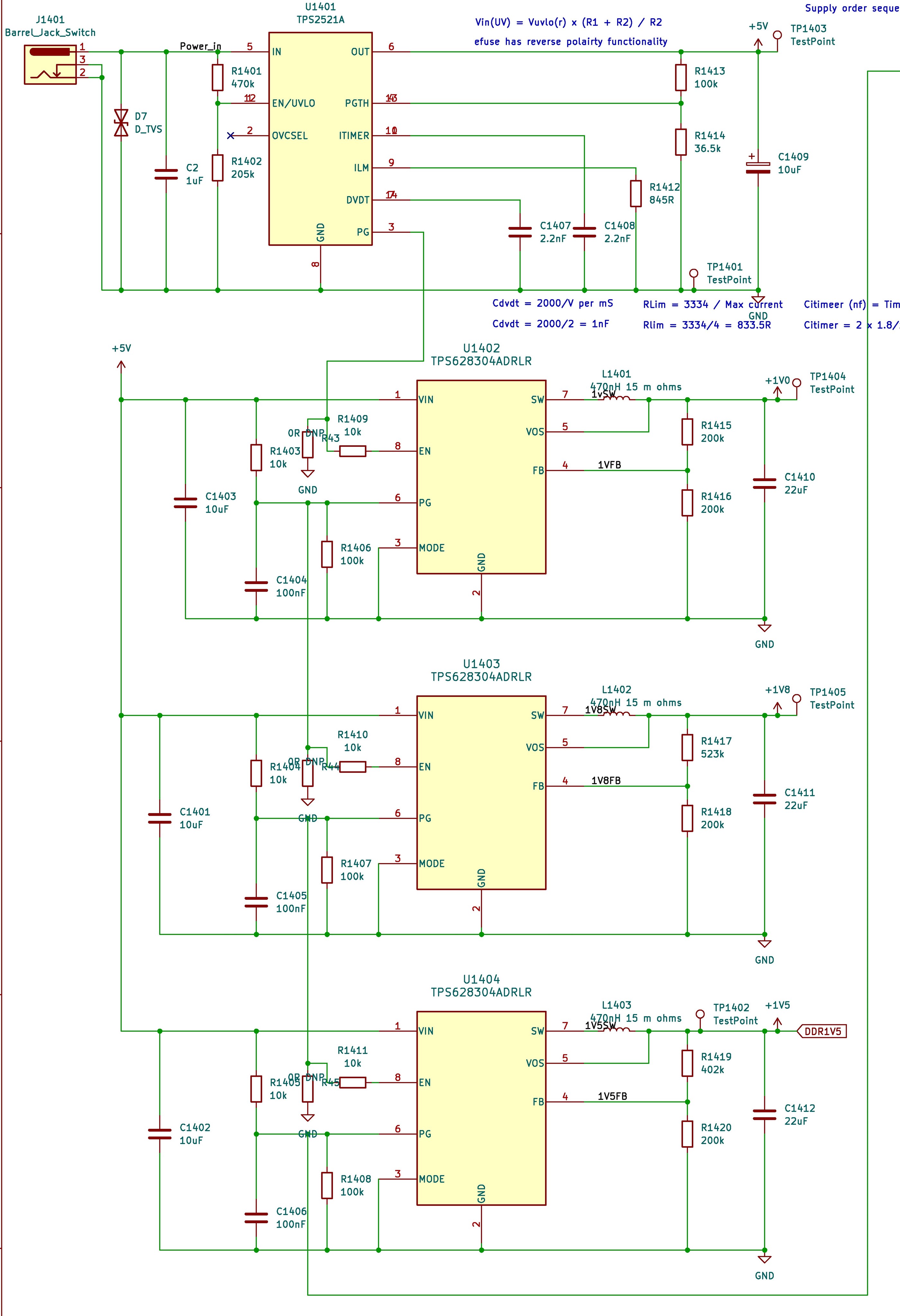
I have multiple TPS628304 to provide multiple voltages in my design. i.e. each TPS628304 will provide one of a range of voltages - 1v, 1.2v, 1.8v etc. Prior to the TPS628304 I have a TPS2521A efuse.
I intended to use the PG signal to feed into the next modules EN so that each of the supplies will power up in sequence one at a time. I have got the board made and I am in the process of fault finding. Looking at the schematic I cannot understand how it would work. Would someone be able to have a look at see what they think? I tried to attached an extract but looks like I can only embed an image in the post.
FYI I have already found that the PG pin of the TPS2521A is missing a pull up resistor to 5v. C1404 and R1406 act as a filter on the PG signal, this design is copied to the other supplies. I have resistors on the EN pin to GND which are for testing purposes and are not populated.
Before the PG of U1402 PG is enabled I would expect to see 5V at the EN pin of U1403 i.e. U1403 is enabled, I say this because R1403 pulls the line high. When the PG output of U1402 is enabled I would expect to see 0V at the EN pin of U1403. I say this because when the PG pin is enabled it is effectively pulled to GND because it is an open collector output. From my understanding of the datasheets this is not correct (EN high = supply enabled and EN low = supply disabled).
I assume I have understood something incorrectly but I cannot see what it is.
Scott

