- Ask a related questionWhat is a related question?A related question is a question created from another question. When the related question is created, it will be automatically linked to the original question.
Tool/software:
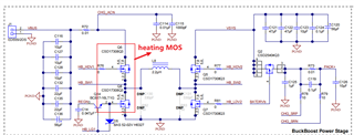
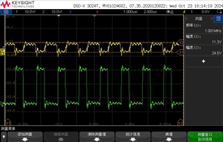
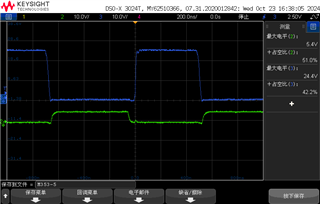
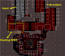
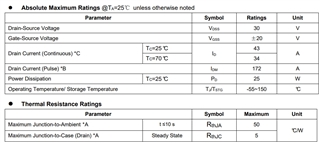
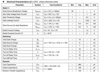
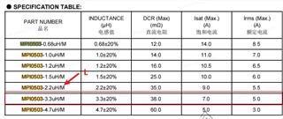
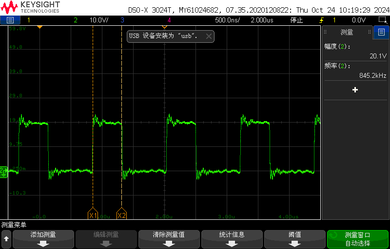
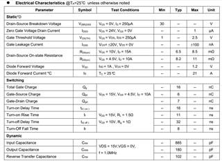
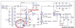
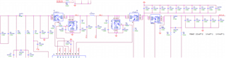
Hello, when I am using BQ25703A to charge the battery, the input voltage is 20V/1A and the output current is around 2A/8V (BQ25703A is soldered onto the board I designed). I found that the two MOS transistors in Figure 1 are heating up severely, probably at 55 ℃. However, when testing the EVM using the same method, the temperature of the two MOS transistors is only 40 ℃. I captured the waveforms of the two MOS gates on the EVM board as shown in Figure 2, and the waveforms of the two MOS transistors on the board I designed myself are shown in Figure 3, but I did not see any significant differences; Figure 4 shows the PCB layout of the board I designed myself ,The input wiring width is approximately 3-4mm, Figure 5 and Figure 6 shows the selection parameters of MOS transistors, Figure 7 shows the parameters of inductors, and Figure 8 shows the waveform of SW pins. I hope you can provide some improvement suggestions.I am looking forward to your answer very much, Thank you very much,