


Tool/software:
Dears,
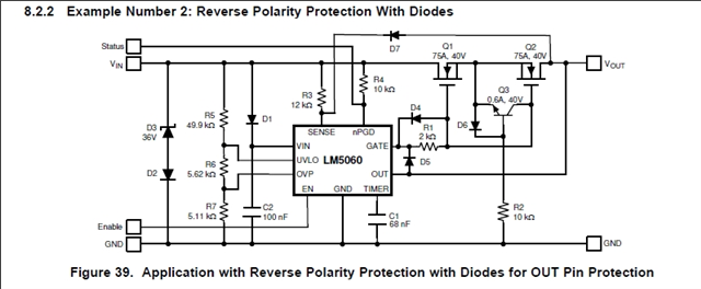
My client used the LM5060 in the controller project. The OVP protection point was set at 49V. During the test, it was found that when OVP was triggered, the voltage at the MOS GATE end would be loaded with 80mA, causing the G end to drop directly to 0. However, due to the presence of capacitance at the MOS SOUCE end, the voltage dropped slowly, causing the negative voltage between the MOS Vgs to exceed the limit and the MOS to be damaged.
After checking the LM5060 data sheet, the client added a diode at both ends of the MOS GS for current discharge. As shown in the figure below and the attached PDF circuit diagram.
The current problems are as follows:
1. When OVP is triggered in this state, the energy at the back end of the capacitor will be consumed by the 80mA internal load of the LM5060. At this time, the LM5060 needs to withstand a maximum power consumption of 4W and an average power consumption of 2W for about 15ms. Since the thermal resistance of the LM5060 is 162.1℃/W, please confirm whether the LM5060 can withstand this instantaneous power consumption and whether it will cause overheating or other faults? If it cannot withstand it, does TI have any other discharge circuit recommendations for the back end capacitor of this device?

2. After the customer added a Schottky diode, the diode leakage current was too large under high temperature conditions, causing the MOS to fail to drive normally and the back end to be powered off. In actual tests under 60°C conditions, the current Schottky diode leakage current is 18uA, which is close to the LM5060 GATE pin driving capability. Can you please confirm whether there is a recommended specification model for diode D5 in the DATASHEET?

See the attached schematic diagram
Many thanks,
Arabella
