This thread has been locked.

If you have a related question, please click the "Ask a related question" button in the top right corner. The newly created question will be automatically linked to this question.

TPS27081A: How to keep Vout off when Vin is ramping up?

Part Number: TPS27081A
Other Parts Discussed in Thread: TPS22995, TPS22916

Tool/software:

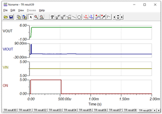
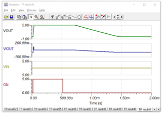
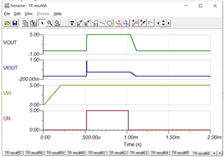
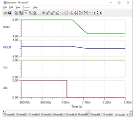
I have a TPS27081A design that I am simulating and I've noticed the following behavior.  If I start the simulation with Vin already established (5V in my case) then I see the part correctly react to the on/off pin (initially the I/O driving the pin is set to 0V).  However, if I start the simulation with Vin=0V and then ramp it up to 5V (all while the on/off pin is still 0V) I see Vout also rise to 5V and stay on.  Its like it is ignoring the on/off pin.  Is the part capable of waking up with Vout in an off state while in the presence of Vin turning on?

  • I thought it might be good to give some additional background info on my application.  I intend to use 3 of these load switches in my design.  All 3 load switch will be powered from the same Vin source.  Only one load switch will be turned on at a time (on time ~2ms), but all will be turned on and off repeatedly over a ~8ms period.  It is critical that the load switches only turn on when the associated on/off signal is being asserted.  Otherwise we will have a high current situation.  We do plan on implementing a discrete active discharge to for each load switch to quickly discharge Vout when a load switch has been turned off

    So based on my initial posts regarding my simulation findings I am worried that this part is not a good fit for my application.  Initially I chose this part due to the flexibility in adjusting the on and off timings.  But this was assuming that it would only turn on in response to the on/off signal.

  • Appending Matt's follow up that he provided to me via email. See below for it:

    "Regarding the start up case.  It appears that the misbehavior is related to how fast the VIN supply turns on and whether there is any resistive load on the output. The TI TINA simulation reference design (SLVMBC9A.TSC) that I downloaded had the VIN connected to a DC supply that did not have to ramp up, it was already full on at t=0.  Also it had a resistive load of 2.4ohms to ground.  This made the circuit work fine.  I proceeded with making changes to the circuit to match my intended implementation.  Vin=5V, Cload=0.2uF, no Rload, R1=10K, R2=1K, C1=10nF.  Our application will also have an active discharge circuit but I didn't initially add it.  Here's an example of the simulation output with the DC source. I understand that Vout is not latched high in this scenario.  It is just staying because there is no load to bleed off Cout.

    Simply adding an Rload=100 shows that Vout bleeds off after ON input goes low.  Here's a pic that shows this.

    Switching out the DC supply for Vin with a voltage generator that has to ramp up shows Vout reacting to Vin before ON changes. It decays off (I'm assuming by Rload) but it still seems like undesired behavior.

    I realized that the ramp rate was set way to fast (10ns).  So I slowed it down to 100us.  However, Vout Still rises with Vin.

    After adjusting different values I found that if I slowed Vin rise down to 200us, decreased Rload to 20ohms, and set R1/R2 to 4.75k/475 that I could get rid of the spike.

    While I'm happy that I got rid of the spike, this is still just a simulation of a circuit.  The fact I had to massage this circuit to get this result is not giving me a ton of confidence in how the part will work in a real design.  So that is where I am looking for TI to chime in regarding this behavior.  Is this a well understood effect?  If so, was my final adjustments the best approach to deal with this?  Is there any other changes I should make to make this more robust?

    One other issue that I am struggling to understand is the discharge behavior.  Based on the eqn #4 in the datasheet, Toff > 2xR1xC1.  So Toff>20us.  With a 20ohm Rload I'd expect the discharge time to take 6us for Cout(2.2nF) to discharge from 5V down to 1V.  So roughly 20us + 6us or 26us.  When I simulate the circuit I see closer to 80us.  Here's a zoomed in pic of the simulation.

    I know the Toff equation uses a ">" and not an "=", but is this much difference to be expected?

    The reason I bring this up is my application is timing sensitive. I only have 300us to shutdown Vout (get below 1V) relative to ON going low.  My current circuit is doing this but the 20ohm resistor is requiring a much larger package size due to power rating than I'd prefer to use.  So is there any other way to make the circuit discharge faster without requiring such a strong Rload value?

    I'd appreciate any guidance you can give to the above questions."

    Marco

  • Hi Marco, Matthew,

    Thank you for sharing this information here. 

    So I am familiar of similar phenomena in some other devices but they have slightly different structure.

    When Vin is ramped up very quickly, It is possible that Q2 FET is turning on for a moment and this is causing this charging at the Vout. If you have a discharge path at output, this gets discharged.

    I have a question, why not use a device with integrated QOD at output. You mentioned that you will implement output discharge in actual application.

    Here is the list of few devices which can handle 5V/3A + adjustable rise time and QOD.
    https://www.ti.com/power-management/power-switches/load-switches/products.html#546=Adjustable%20Rise%20Time&1685=2.7%3B15&2192=Quick%20output%20discharge&238max=5.5%3B23&

    Best Regards,
    Arush

  • For this first prototype design I am trying to keep maximum flexibility not only in being able to adjust the on/off timing of the load switch but also in discharge circuit in order to conduct various experiments with our initial ASIC.  That being said I am planning on including a stuff option of a load switch w/QOD (likely TPS22995) for this first prototype. 

    Our production design won't have the space for the TPS27081 + discrete discharge.  So we will likely use TPS22995 or TPS22916, depending on the max current specs of our production ASIC.

  • Hi Matthew,

    When you simulated this, did you also probe the R1 and ON pin of the device. As I mentioned earlier, I am suspecting that due Q2 turning on for a moment, we are seeing this issue. Did you force ON to low? 

    Another possible reason can be error in simulation model but this is less likely. I feel that it will be best if we test this on the actual hardware (like our EVM).

    keep maximum flexibility not only in being able to adjust the on/off timing of the load switch but also in discharge circuit in order to conduct various experiments with our initial ASIC. 

    For the other devices which I mentioned above, you can adjust on time by changing the slew rate and also the off time by adjusting the QOD resistor value. Since you will prefer integrated solution in the final product, you should directly evaluate on these newer devices. I should be able to provide you some specific testing based on your conditions with TPS22916 if you want. It is difficult for me to test with TPS27081 (as I don't have EVM with me).

    Best Regards,
    Arush