This thread has been locked.

If you have a related question, please click the "Ask a related question" button in the top right corner. The newly created question will be automatically linked to this question.

TPS7A57: Why is there only 1 ground pin? Will this not lead to thermal issues in the example PCB design?

Part Number: TPS7A57

Tool/software:

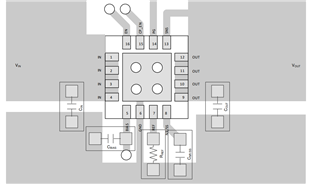
As can be seen in the picture here above, there is only 1 ground pin, pin #6.


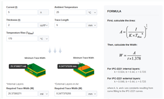
As can be seen on PCBWay's trace calculator, a trace this thin with 5 A of current passing through it will produce a temperature rise of 170 C on top of the 25 C ambient, leading to a total temperature of 195 C.

Assuming the footprint pad has 0.254 mm of width, will this not lead to thermal issues if we go all the way up to 5 A?
Should adding multiple vias under the pad not be recommended instead?

  • Hi Jan,

    The 5A current flows through the internal pass MOSFET to the load, but the return path does not flow through the internal LDO circuitry.  In LDO's, the return current flows through the ground plane of the PCB back to the input source.  The GND pin of the LDO only needs to handle the small quiescent current needed to operate the LDO (mA's of current in this case).

    The circles shown in the center ground pad of the TPS7A57 are intended to be thermal via's.  These vias are attached to the thermal pad which help dissipate heat from the device.  The thermal pad should be tied to GND.

    Thanks,

    Stephen