TPS54519: SW undershoot at max load.

Part Number: TPS54519

Tool/software:

Hello TI support

I've got an issue to meet the specification of the PH pin of the TPS54519, especially the "undershoot" as following:

The max abs rating is -2V during 10ns.

My converter operates from 3.5V to 0.95V 5A and has the following undershoot:

CH4 : total output currrent (250mA is not included in this trace)

CH2 : output voltage (AC coupled)

CH1 : PH pin
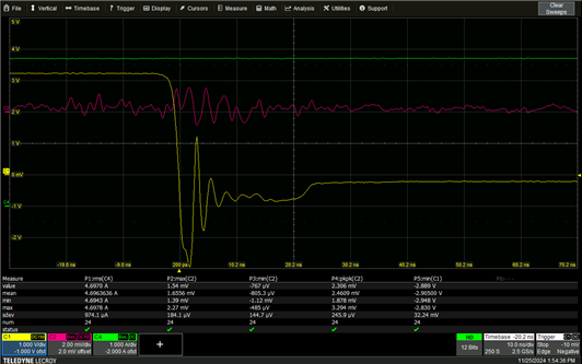
(min with stat = -2.95V).

The probing is made with a 1GHz scope, 500MHz passive 1:10 probe with a small pigtail (for the GND connection).

The layout is the same as the EVM.

The only way to achieve the specification with margin is to add:

- A RBOOT of 33Ohm

- a high and low side snubber of 2.2Ohm and 2.2nF
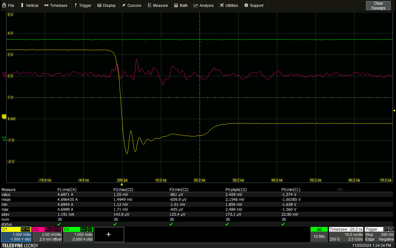
(min with stat = -1.64V).

Could you confirm :

- the undershoot measured (with no snubber) is really an issue regarding the max abs ratings ?

- the way to fix it is correct and sufficient ?

The layout and schematics could be provided by email for more detail.

Thanks for your support

  • Hi Lionel,

    this exact topic is covered in this app note: slva494a.pdf

    It seems that your measurement method is already pretty good (short GND connection, etc)

    The short answer is: During normal switching operation, going below the negative limit is no issue. The detailed explanation can be found in the app note.

    I hope this answers your question.

    Regards, Werner

  • Hello Werner

    Thanks for this app note and your support.

    I was aware that the -0.6V on the TPS54519 MAR was for a static outside source and I was also aware of the behavior during dead time of HS and LS MOSFET.
    I used proper grounding (spring short pigtail as in the ap note with GND on PGND of the chip) with high scope bandwith. To compare I also use a 1GHz active probe (with short GND lead). The waveform was exactly the same.

    However, for me, the mention -2V 10ns transient was especially to specify the max undershoot during body diode "frewheeling".
    In the app note, it's not 100% sure if we have for instance -5V 20ns on SW is there a potential issue with the chip lifetime .

    It says it's ok if we use good layout technic but nothing to really quantify and put a limit.

    A lot of TI forum members seem to share the same fear as me :

    Thread1

    Thread2

    Thread3

    Thread 4

    Some TI FAE pointed out the "transient 10/20ns MAR", some say the "energy is limited during 10/20nss".

    So I will check the efficiency with and without HS and LS snubber. And also do radiated/conducted emission test. Then I will make a choice to keep them or remove them with all the testing information.
    For the output ripple, with the 2 snubbers, the "HF noise" is greatly reduced.
    What do you think about this procedure to make the final choice ?

    Thanks for your support
    Best Regards

    Lionel

  • Hi Lionel,

    in general, if your system can allow for the snubbers, include them.

    The FAE is correct, any undershoot created during normal operation is limited in energy and usually no issue at all. Even when following all best practices for the measurement, you still have parasitics that will show a  worse noise than what is actually in the system.

    The -2V is a hard limit for any externally generated noise on the SW line, because then you cannot guarantee the energy in that noise and the impact to the device.

    Also, please share the results of your tests.

    Regards, Werner