This thread has been locked.

If you have a related question, please click the "Ask a related question" button in the top right corner. The newly created question will be automatically linked to this question.

TPS543C20: Internally compensated ACM

Part Number: TPS543C20


Tool/software:

Hi Experts,

Asking your assistance on TPS543C20's internally compensated ACM. From this presentation:

From page 22 about VCOM, user may think its DCV would be around 1-1.2V. Questions to follow below:

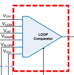
1. Figure on page 14 shows the negative sum signal is V NEG, which is equal to V CVI plus VCOM plus V S/H. Is there an error here? Should V CVI be V CtrI?

2. On page 13, customer is very interested in how the DC feedback help increase the phase margin around the double pole. Is there any reference document to share?

Thank you for your guidance.

Regards,
Archie A.

  • Hello Archie,

    Please allow some time for a response as there is a delay due to TI Holiday.

    Thank you,

    Calan

  • Hi Archie, 

    For #1, you are correct. Vcvi should be Vctrl, as the inputs to the loop comparator are as follows

    For #2, I will check if there is any reference material to share. As of now, I do not have any

    Best,

    Britton

  • Hi Britton,

    Thank you for responding.

    Looking forward hearing your confirmation on point #2.

    Regards,
    Archie A.

  • Hi Archie, 

    There is no reference document that I could find but here is some more details about that - 

    The inductor resonance is dictated by a repeating process of a voltage differential across the inductor and the inductor creating a current to cancel that voltage differential. When there is zero voltage differential across the inductor there is a non negative current, this requires a negative voltage differential to remove. When the current through the inductor is zero, there is a non zero voltage across the indcutor. This repeats over and over to create resonance. 

    When we add the current feedback into the control loop the voltage that is forced across the inductor is reduced - therefore there is less current when the voltage differential is zero and less voltage differential when the current is zero. This lowers the Q factor.

    Ultimately, the DCI feedback is creating a finite output impedance to the SW voltage source on the inductor

    Best regards,

    Britton