This thread has been locked.
If you have a related question, please click the "Ask a related question" button in the top right corner. The newly created question will be automatically linked to this question.
Tool/software:
HI team,
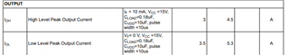
UCC23513 gate resistance is calculated by below equation, said by datasheet.
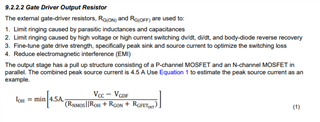
However, 4.5A is the peak output current as typical. Should customer uses 3A to calclurate it? Or this variation is not a value of device by device variation, is it condition dependence?
Regards,
Hayashi
Hi Hayashi,
The typical value should be used. The minimum datasheet spec is recommended by the design simulations which incorporate worst case temperature and process variation combined.
Here is the typical IV curve for an output pull-down NMOS at DC. As you can see, the output current depends on the Vds, which is the voltage between the OUT and the rail. When the Vds is high, it acts like a current source, and when Vds is low, the output acts like a resistor.
However, output current does not change instantaneously into a 5A current source. Here is the output current (Igate) of the UCC23513 and several P2P gate drivers while driving a IKW30N65ET7 IGBT with an external resistor of 1Ω vs 20Ω. As you can see, the gate drivers do not reach their DC Iout peak ratings of 3-5A.
The shaded regions represent the periods of switching loss. In this region, Vds is low. Therefore, the Roh is a more significant specification than peak Ioh to compare drive strength, expecially when higher Rg is used.
Best regards,
Sean