Tool/software:
Hi all / Mulin Yuan
My previous thrad was locked due to timing. I have now had chance to update this design. Please could you have a look and check if everyhting now looks ok! Thank you!
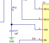
Schematic: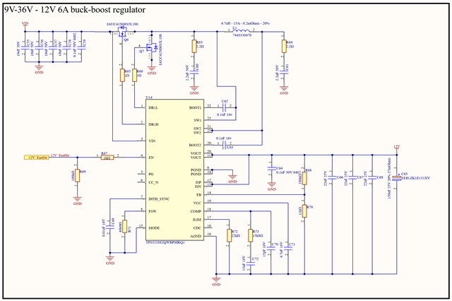
Supply input caps before the ones above: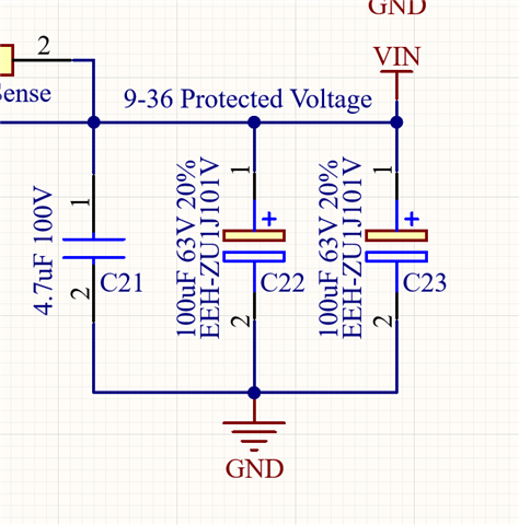
3D view: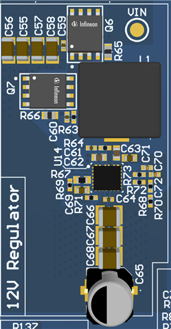
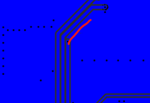
Top layer:
Inner 1 GND layer:
Inner 2 also GND layer:
Bottom layer:


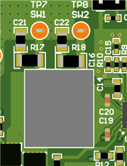
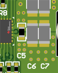
Closer images of IC region:


Thanks in advance!