This thread has been locked.

If you have a related question, please click the "Ask a related question" button in the top right corner. The newly created question will be automatically linked to this question.

TPS65988DJEVM: TPS65988DK

Part Number: TPS65988DJEVM
Other Parts Discussed in Thread: TPS65988DJ, TPS65982, TPS26750, TPS25751, TPS25751EVM

Tool/software:

Subject: Urgent: TPS65988DJEVM Failing During Testing

Dear Team, I recently purchased two TPS65988DJEVM boards and conducted a test using a USB-C sink to receive 5V. I then applied a 3A load with an active load to verify its stability overnight. Unfortunately, the EVM failed within less than an hour.

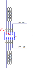
Upon inspection, we found that the board had burned out, with the D4 diode on Port A damaged(pin A and C short ). We attempted to replace the diode, but the port remained non-functional, likely due to additional component failures.

We then conducted a similar test on the second board purchased at the same time, this time sinking 15V, but it also failed within approximately one hour. Again, D4 and other unidentified components were damaged. At this point, we are unable to proceed with further evaluation. Could someone assist in identifying why the EVM cannot sustain power delivery for more than an hour? Any insights into potential causes and solutions would be greatly appreciated. Thanks,

Steve

  • Hi Steve,

    Is there a reason you are evaluating the TPS65988DJ? Are you using an Intel Reference design using this part? If you are not using an Intel reference design, we do not recommend using this part.

    You are seeing the D4 resistor on the VAR DCDC path burning out? That is a 30-V Schottky, I would not ever expect that node to exceed 20-V and would not expect it to burn out. Did you change the EVM configuration at all?

    Where are you drawing power from, where is the E-load attached?

    What is your configuration of the J11 jumper?

    Under normal operation, I would not expect the EVM to fail if you are just drawing a load at 5 or 15-V.

    To be safe, I would recommend removing the PA_PP_EXT -> sink side pA jumper and directly draw load off of the J11 pin 1 pin. This should disconnect the sink path from the SYS_PWR node and hopefully avoid any connection to the D4 resistor.

    Thanks and Regards,

    Chris

  • Hi Chris,

    Thanks for your prompt reply. We are not using this in an Intel-related design. Instead, we are using it for a USB-C PD hub with UFP or DFP data ports, which gives us more flexibility for future projects. In fact, we have been using the TPS65982 since its launch.

    The J11 settings were left at their default values—we did not make any modifications on either board. We simply added a load to the USB-C port, allowing it to sink power at 5V or 15V. Have you conducted a similar test where you leave it running for an hour with a 3A load?

    Our input power is 20V, so I don’t believe it would damage the 30V D4 diode. However, the issue still occurs. What are the default PDO settings? Based on my tests, they appear to be 5V, 9V, 15V, and 20V—are they all limited to 3A?

    By the way, is it possible to export the configuration from the EVM so we can modify only the necessary settings? There are so many parameters to configure if we start a new project from scratch using the Configuration Customization Utility.

    Steve

  • Hi Steve,

    What requirements do you have for your Type-C PD needs for future projects? I would like to make sure you have the correct IC for your needs.

    We will not support use of the TPS6598XDJ parts for any non-Intel designs, so you would need to use a different IC. The main ones we are currently offering are the TPS25751 and TPS26750.

    We simply added a load to the USB-C port, allowing it to sink power at 5V or 15V

    Oh, that makes more sense, I misunderstood that the 988 was sinking. It sounds like it is sourcing 5/15V at 3A.

    Have you conducted a similar test where you leave it running for an hour with a 3A load?

    I don't know the full history of the EVM, but checking with a couple engineers, it's unlikely we stress tested it like this. I'm not personally aware of a similar test. The EVMs are designed for general functionality and evaluation, but not necessarily for characterization and extended test.

    Our input power is 20V, so I don’t believe it would damage the 30V D4 diode.

    Yeah, I completely agree here.

    Is the D4 diode the only thing damaged? It seems to be safely rated for both the Voltage and current in mind. The Diode has an avg forward current of 5-A, which should be fine for 3-A loads. It does seem a little close for the 5-A case, but your testing is currently at 3A.

    Have you been able to determine what else is not working/got damaged? Is it isolated to the DC-DC converter for sourcing?

    If one of the secondary ports on the EVM is working, could you try running the load test for 15-20 min and put a temperature gun on the EVM to see what is heating up? It may help to identify what is breaking down.

    What are the default PDO settings? Based on my tests, they appear to be 5V, 9V, 15V, and 20V—are they all limited to 3A?

    Unfortunately, I can't find the original pjt for the EVM and do not have a new 988DJEVM on hand. You best bet might be to use the "import settings" option described below.

    Typically we will set up the configs to support up to 5-A for the 20-V PDO. (Typically 5V/3A, 9V/3A, 15V/3A, 20V/5A). You may not be seeing 5A at the 20V PDO if you are using a cable that is not rated for 5-A. We do limit advertised sourcing capabilities depending on the cable capabilities. 

    The TPS6598X family does not support source voltage greater than 20-V, and the feedback is purely resistive (no I2C or other programming of VOUT), so I can't imagine the voltage to ever exceed 20-V.

    By the way, is it possible to export the configuration from the EVM so we can modify only the necessary settings? There are so many parameters to configure if we start a new project from scratch using the Configuration Customization Utility.

    Which GUI are you using? Some GUIs have a "Device->Import Settings From Device" option that may fit what you need. You first need to go to "Adapter->Configure Adapter settings" and make sure a valid USB to I2C/SPI adapter is selected.

    Thanks and Regards,

    Chris

  • Hi Chris,

    Our projects require switchable resistive feedback pins for the BUCK, the ability to function as a power source for charging UFP or DFP devices, MUX control via a USB orientation GPIO pin, and customizable PDOs.

    I have reviewed the TPS25751 and TPS25751S. Do they support above requirements? Can the TPS25751 internal MOSFETs continuously support 5A?

    Best Regards,


    Steve

  • Hi Chris,

    Does the TPS25751 require an external SPI flash for its firmware? If not, does that mean its firmware is fixed and cannot be customized using your tool?

    Best Regards,

    Steve

  • Hi Steve,

    Unfortunately the TPS25751 is not meant for source only applications and is probably not a good fit here.

    If you are ok with the PD controller not being up to the latest compliance, you can consider the TPS65988DDK. The version of compliance it was designed for is almost obsolete so you will not be able to achieve USB-C PD compliance with this part, but it is PD capable and will work with newer device as the spec is backwards compatible.

    Thanks and Regards,

    Chris

  • Hi Chris,

    I understand it is for power bank applications. For source only applications, we needs to switch the USB MUX. Besides, does TPS25751 support resistive switchable resistive feedback pins for the BUCK as TPS65988DJEVM?

    Steve

  • Hi Steve,

    Correct, the TPS25751 is meant for battery charger applications and for DRP and Sink only applications. One of the issues with sourcing is that the TPS25751 requires a 5-V rail (PP5V) in addition to the PPHV power supply for sourcing various voltages. The TPS25751 is also not currently supporting Source only configurations in the GUI used to generate FW images.

    By viewing the "GPIO Events" section in the TPS25751 TRM, you can see the configurable

    For source only applications, we needs to switch the USB MUX.

    Yes, the TPS25751 has a GPIO event for cable orientation typically needed for USB muxing

    Besides, does TPS25751 support resistive switchable resistive feedback pins for the BUCK as TPS65988DJEVM?

    Yes, It should have the same events. The SourcePDOxContract ones are individual GPIOs for each PDO. The SourcePDOContractBitx ones 

    Thanks and Regards,

    Chris

  • Hi Chris,

    Based on the information you provided, I believe we can use the TPS25751 in our applications since we can supply 5V for the 5V rail. The DRP mode shouldn’t be an issue if it is set to "Try Source First," correct?

    By the way, is the firmware stored inside the chip itself, or does it require an external SPI flash?

    Steve

  • Hi Steve,

    The DRP mode shouldn’t be an issue if it is set to "Try Source First," correct?

    Yes and no, It should help, but won't necessarily guarantee the port always enters as a source if the other port is in a similar configuration.

    By the way, is the firmware stored inside the chip itself, or does it require an external SPI flash?

    No, the FW is not stored inside the chip itself. The TPS25751 requires an external I2C flash. See U6 on the TPS25751EVM.

    As mentioned before, the issue with the TPS25751 is that it does not support >5V only source only configurations, and I am not aware of a timeline for adding this support. This would prevent you from generating an image for the IC from the GUI.

    Thanks and Regards,

    Chris