A related question is a question created from another question. When the related question is created, it will be automatically linked to the original question.
If you have a related question, please click the "Ask a related question" button in the top right corner. The newly created question will be automatically linked to this question.
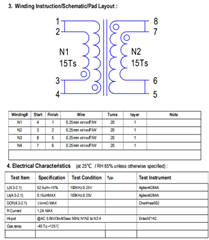
-Firstly, could you please share your Design Calculator tool used for your schematic design. Could you also share the DS of your transformer? I need to verify Lmag and turns ratio.
-I recommend adding a snubber between VIN and SW to attenuate the HF harmonics that come from the clamp peak at the switching node voltage. You can use a 100ohm+100pF.
-TC: if you are just testing at Ta ambient 25C, you can just leave this pin floating. If testing at different Ta, I recommend using TC resistor at TC pin to compensate the VF forward voltage variation coming from secondary diode.
-Regarding the layout:
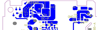
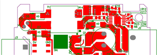
1. EN, RSET, SS, COMP pins: I recommend adding a signal ground plane for the return paths of all these pins and isolated from bigger GNDP plane and make the connection through the AGND pin to the thermal pad (this last is already done). This improves regulation (return of COM pin) and return connection of signal pins. If possible place all components of these pins at one side of the IC away from the switching and power pins. See example below from EVM layout.
2. Place MOSFET on top layer and place it next to the transformer. Avoid using vias in the main switching loop (VIN, xfmr, MOSFET) as they introduce parasitic inductance that can generate voltage drop and affect regulation. You can place D6 and D8 clamp circuit on bottom layer to get more space. See example below from EVM layout. This is important to keep the switching loop as short as possible and improve regulation.
3. Place a wide and big GNDP plane over all the available space at the primary side. This ground plane needs to connect return of the input caps VIN and the return of Rcs resistor (primary switching loop). See example below from EVM. This ground plane helps not just for good thermal performance but for low EMI to mitigate any residual H field coming from leakage inductance in the transformer.
4. Place a wide and big GNDS plane over all the available space at the secondary side. Same idea than above. See example below from EVM
Regarding the output ripple, could you please take the switching waveform in parallel with AC Vout? Also, wat are the load conditions tested, is this at no load or light load? VIN tested? I suspect that those large HF peaks at Vout AC come from EMI coupling to Vout due to the layout.
Attached are our calculations and transformer data mentioned as required.
In addition, we found in the test that the ripple is divided into two parts, one part is the triangle wave of 25kHz that the switch normally oscillates, and the other part is the sudden voltage of more than 1M.
The abrupt voltage can be reduced by adjusting the MLCC of the back end, and the triangular wave can be reduced by increasing the inductance and filtering capacitance of the output.
Therefore, we plan to increase the filtering capacitance of 2200uF at the output end, and increase the high-frequency filtering of 10uF, 1uF and 10nF at the same time.
At the same time, improve the current loop and ground wiring according to the following suggestions.
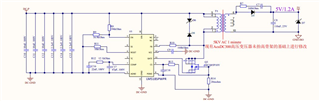
-UVLO: resistors are set for UVLO_on 18.8V and UVLO_off 17.2V. In your calculator I saw Vin_min=9V, which is lower then UVLO thresholds. Please check those values or confirm Vin_min.
-FB: Please update FB resistor to 54kohm. This value comes from the reflected Vout 5V and Rset 10kohm Vref=1V.
-RC filter at Rcs: I cant see the values in the schematic. I recommend using 100ohm+100pF filter.
-MOSFET: Use an N-channel, not P-channel. Gate driver of LM5185 is designed for N-channel.
-Compensation network, Lmag and Nps look good.
-Regarding the ripple, are you measuring Vout ripple, correct? You can use HF decoupling caps such as 10nF at Vout and also lowe frequency filtering caps such as 10uF-1uF. I agree on the switching loop, this can be done placing ground planes and spread them over the available space as recommended below.