Hi,
I would like to ask some questions with TPS6507x's wLED boost and TPS6023x LED drivers.
The Design of LED Driver
LED drivers on TPS6507x and TPS6023x all have at least two current sinks, but with only one VOUT.
In addition, the required current for current sink(s) has only one value at the same time. Although for TPS6507x there can be two resistors at ISET1 and ISET2, which of them is used is determined by [Bit 7, WLED_CTRL2] and this provision is for enhanced PWD dimming precision.
Then we face the problem of boosting VOUT so that DX current for some or all DX sinks are satisfied. This might be nontrivial depending on the design of LED boosts.
The carefree case

When the paths from VOUT to different DX's have the same LED connection (both forward voltage and V-I curve), then they can naturally be connected in parallel. This is the trivial case and does not demand much knowledge of the LED driver's internal design.
Design Variations
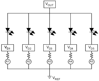
When VOUT-DX connections are not balanced, it might be impossible to satisfy current requirements at all DX's at the same time. Therefore, I guess the actual design might be to require one of the four conditions below:

In the diagram I reduce the number of DX Ampere meters (or functionally equivalent components) to two for simplicity, however the principle extends naturally to >2 numbers.
The LED driver might monitor only one of sinks, or an incomplete set of them. For example, TPS60230 datasheet Fig.12 show D5 unconnected:

And this corresponds to "ONLY" or "OR" design above.
The LED driver might also monitor all DX sinks. For example, TPS6507x datasheet page 64:

And this corresponds to "AND" design above.
Initial Conclusion: TI LED drivers employ different current monitoring schemes, as evidenced by the two examples above. This observation justifies the need for the following discussion.
We consider different cases:
AND sinks with fixed DX

If the voltage at each DX is fixed, then unbalanced parallel connections might lead to problem. Basically, the resistance of different VOUT-DX paths can be different, so it's impossible to expect same sink current for different paths.

If we require each IDx ≥ ISET, then when current on the path of least resistance has already reached ISET, current on other paths are still below ISET. VOUT still has to increase, and the consequence might be that the LED breakdown voltage of the path of the least resistance be exceeded.
To prevent this from happening, one solution (perhaps the only) is to add resistors in each path(s) to balance the resistance. The value is calculated as in the diagram below:
AND sinks with Adjustable DX

We might also design a more sophisticated and "intelligent" LED driver which automatically accommodates unbalanced paths. The key of this design is adjustable DX voltages for different sinks.

At the beginning, all DX's have the same voltage. As VOUT increase, the path of the least resistance (D1) will first reach ISET. The voltage drop on this path cannot be increased further, or breakdown condition might happen.
To maintain this voltage difference, VD1 increases along with VOUT. VOUT will eventually rise to a level such that the current on path 2 also reaches ISET while VOUT-VD1 remains unchanged. If there are more than one paths, the same procedure would continue until eventually the path of the last resistance reaches ISET.
Although in principle this handles all types of connection even including unconnected pins for which VOUT will eventually stop at its maximum possible value, I believe it is NOT implemented on TI LED drivers. Because for each DX, an additional charge pump needs to be added to increase its voltage along with VOUT.

For TPS60230 its Functional Block Diagram shows only one charge pump. If adjustable voltage implemented for each DX, there would be six charge pumps in total, greatly or significantly increase the host. This will rule out its practical application.
ONLY sinks

This design is much easier to implement, and would have no problem with disconnected DX pins.
ONLY/OR sinks

This design is similar in effect to "ONLY" design above.
Incarnations on TPS6507x and TPS6023x
TPS6507x wLED boost
Datasheet page 64:

So this must the "AND" type. It should not have adjustable DX pins due to cost consideration.
TPS60230
Datasheet example show pins unconnected ⟹ must be among {ONLY, OR} type; cannot be "AND" type.

TPS60231
I cannot infer which sink current type it uses from datasheet examples.

Question

I asked a question in TPS65070: One string of LEDs which TI employee Daniel Acevedo advised me to tie ISNK1 and ISINK2 together. I could not understand the reason for doing this hence the above discussions.
Could anyone give detailed and affirmative comments on the above points?
Zheng

