This thread has been locked.

If you have a related question, please click the "Ask a related question" button in the top right corner. The newly created question will be automatically linked to this question.

UCC21520: Noise Immunity

Part Number: UCC21520
Other Parts Discussed in Thread: UCC21530

Tool/software:

Team, 

Since customer found that both INA and INB pin have some ripple noise during power-on, it could damage MOSFETs of the half-bridge. With this ripple voltage, the INA or INB pin would be possible act as HIGH level to lead to output is switching.

Question: Customer asked if there is a 10K-Ohm resistor connected in parallel from INA/INB to GND pin as a pull-down resistor for better noise immunity (not verify yet). Is there any side effect or risk? Very thanks. 
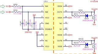
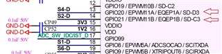
GPIO21 (S2-D, INA)

f

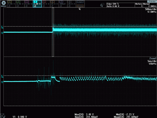
Issue: MOSFETs are shorted thought together. Customer is still doing investigation for the root cause now.

Application: 1-phase String Inverter

  • Hi Brian,

    The outputs have a parallel active pull-down circuit that will hold both of the outputs LOW during power-on. The inputs also have 180k Ohms of pull-down resistance to make sure they are set low if the input is high-Z during start-up. Adding a local decoupling capacitor of 100pF-1nF will also help filter input noise if it is a concern. There is also a 12ns de-glitch time-domain filter that will ignore transient pulses, even if they exceed the input threshold voltage.

    Did your customer observe the output of UCC21530 drive high to VB+ with a square wave? This would be clearly visible if input noise did indeed cause the output to turn ON.

    If not, the Mosfets could be turning themselves on due to Miller injection through the parasitic Cdg. When high dV/dt is applied across the drain and source of a MOSFET, current can be injected into the gate. It is very important to clamp this current injection with a low-impedance to the Mosfet source. In your circuit, there is both a diode and 6.8 Ohms of impedance between the gate and the pull-down network of the gate driver. This may be enough resisance to cause a Miller injection hazard.

    My recommendation would be to move the diode to the turn-on path, and use 0 ohms of turn-off resistance to prevent a Miller injection hazard. Also, you should see if it is possible to reduce the start-up dV/dt across the half bridge by increasing the HV decoupling capacitance.

    Best regards,

    Sean

  • Hello Sean, Thaks for comments.

    In the d/s, it says the CIN is suggested between 10pF to 100pF for the filter design. But you mentioned it can be 100pF - 1nF. that could cause the propagation delay during switching. Customer experienced the failures many years ago, there were damages on the same converter with 1nF cap for CIN. therefore Customer is concern to put higher input cap. 

    For the behavior of the device outputs, we'll double check if there is a fault turn-on or not during power-on?

  • Hi Brian,

    A larger input capacitor will have a lower impedance, meaning that the voltage rise will be lower for a given noise current injection. A larger capacitor will add propagation delay if the input resistor remains 51 ohms, but you can reduce the input resistor to achieve the same propagation delay.

    If input noise did cause the output to turn on, you should see a square wave at the output. If the Vgs is more of a small triangle wave, then the root cause is more likely to be start-up Miller injection, and a lower impedance Vgs turn-off loop is needed.

    Best regards,

    Sean