This thread has been locked.

If you have a related question, please click the "Ask a related question" button in the top right corner. The newly created question will be automatically linked to this question.

TPS65279: Strange behaviour on PGOOD pins

Part Number: TPS65279

Tool/software:

We have used the TPS65279 successfully for several years (using thousands of TPS65279). But recently we made a minor change in the layout and now we have problems with 70 % of the boards. I have not found the exact problem yet but while investigating I found a strange behaviour with one of the TPS65279 that are used on the board.

The PGOOD signals (or at least one of them, they are soldered together) from the TPS65279 sometime rises before the output voltages are valid:

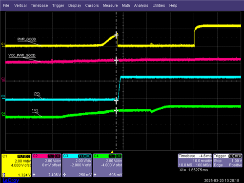
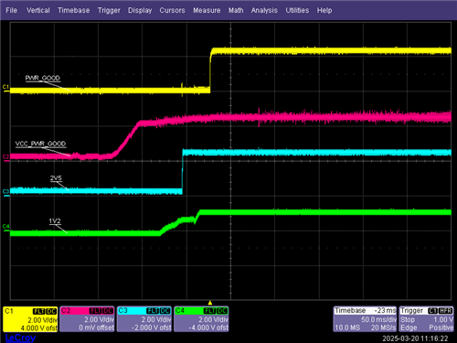
The normal behaviour looks like this (note that the horisontal scale is slightly changed):

The schematic looks like:

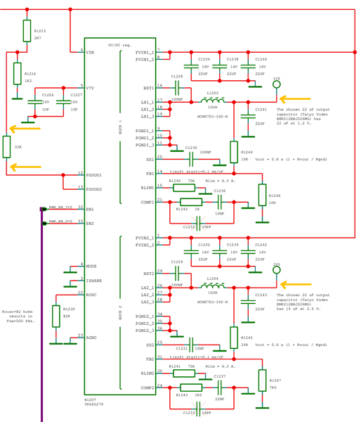
VIN is 12 V. The yellow arrows indicate where the oscilloscope probes are placed.

The "glitch" on PGOOD is temperature sensitive. It almost always occur when the board has been powered off for a few minutes. But after running the board for perhaps 10 seconds it almost never occur. The current drawn from the 1V2 and 2V5 rails is very low when the board is being powered on, probably below 1 A.

  • A note on the PGOOD signal in the schematic above: This is how I have connected it while measuring. In the design the PGOOD signals are connected to a hardware reset circuitry.

    So what I would like to know is why PGOOD behaves like this (rising before output voltages are ok depending on temperature).

    I should also mention that cooling the TPS65279 with cooling spray has the same effect as letting the board be powered off for a while.

  • I have now also made a mesurement on the enable signals to the TPS65279:

  • Dear Sir,

    Pls kindly let me check your question and get back to you during these days. Thank you!

    BRs

    Lucia

  • In the first oscilloscope screenshot it can be seen that the 1V2 rail starts to rise before the TPS65279's 1V2 enable pin was set high. I therefore disabled the regulator that caused this but it did not seem to affect the behaviour:

  • I have now measured the voltage on the COMP1 and COMP2 pins. They are 0 V when the "glitch" on PGOOD occurs.

  • Dear Sir,

    Thanks for your further update. I will check your question during these days. Thank you!

    BRs

    Lucia

  • Another question: How much current can PGOOD sink? I can't see that specified in the datasheet.

  • Dear Sir,

    Could you pls also kindly share me the layout before and after? Thank you!

    BRs

    Lucia

  • Hi Lucia.

    We have now found out why the new batch of boards fail. There was a manufacturing fault that caused the power sequencing to be out of order. This is the reason why we have problem with the "glitches" only on the new batch. Tomorrow I will see if the problem exists also on older batches.

    So the original problem still exists; why is TPS65279 generating a "glitch" on its PGOOD output(s)? This is something only you at Texas Instruments can answer since you know how the TPS65279 looks inside. Please note that we see this problem at room temperature on about 70 % of the boards, Also note that it is temperature dependant, cooling/heating the TPS65279 makes the "glitch" come and go.

  • Ti told me via mail:

    Until the EN pins or VIN aren’t high and present, there is no valid usage of the PG pin and it’s outputs.

    Case 1 – VIN is high/Low, EN is Low – PGOOD is invalid

    Case 2 – VIN is low, EN is high – PGOOD is valid and would be low

    Case 3 – VIN is high, EN is high – PGOOD will go high after FB voltage goes above 94% of the target value.

    This is an answer I accept. But I suggest that such importnat information is stated in the datasheet.

    Regards