This thread has been locked.

If you have a related question, please click the "Ask a related question" button in the top right corner. The newly created question will be automatically linked to this question.

UC3825A: Possible spice model mistake?

Part Number: UC3825A
Other Parts Discussed in Thread: UC3825, UC1825, TINA-TI

Tool/software:

Hello everyone,

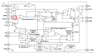
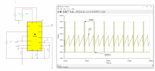
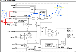
I have an issue with the UC3825 spice model (well the UC1825 that is provided on the UC3825 page), the issue is that on my simulation when I expect the PWM to be off I see some output, this is when EAout is 0V... when looking at the block diagram, I see that between the RAMP pin and the comparator is a voltage source with the negative side on the RAMP pin... if i look into the spice model, the negative side of the source seems connected to the comparator... V4          RAMP 22 1.25.... looking to other sources below, the arrangement looks ok....  V2          26 GND 1

Please advise.

Best Regards.

  • Hello Abel,

    We are reviewing your question and will respond shortly.

    Regards,

    Jonathan Wong

  • Hello Jonathan,

    Thank you... just as info, a colleague pointed me to the SG3825 datasheet, very interestingly/annoyingly its block diagram shows the cell on the same direction as the UC3825, but it also adds the polarity signs on the opposite direction, what can I say... the UC3825 doesn't include the signs... now, assuming the polarity is ok, I still don't think the PWM should be ON when EA_Out is at 0V (the CT reference on the comparator will be offset -1.25V from the 1V which is the lowest of the CT signal, ending on -0.25V on the comparator input)...

    I will be making some measurement today to get more insight on this peculiarity, besides the simulation...

    Best Regards.

  • Hello Abel,

    Do you have a TINA-TI file with the UC3825 that you can share?

    Regards,

    Jonathan Wong

  • Hi,

    That 1.25V is to help avoid RAMP valley noise uncertainty. So when EAOUT=0, RAMP needs to reach > 1.25V to terminate the pulse (the right of 1.25V to become > EAOUT =0), but CLOCK falling edge already set up OUTA or OUTB pulses, so EAOUT =0 cannot make 0 pulses. 

    RAMP typical valley 1V, so needs to increase about 0.25V to reach > 1.25V to make PWM non-inv > EAOUT =0. The OUTA or OUTB pulse starts at RAMP valley and CLOCK falling edge, from valley (1V) to 1.25V, OUTA or OUTB will show pulses.

  • Hello Jonathan,

    Below the file of the model and an example where Im trying to understand the behavior of the device, the picture shows the device giving output with EAOUT 0V. CT on the picture is what I expect, due the internal oscillator compares against 1V and 2.8V, so adding 1.25V will raise the CT signal to 2.25V at the input of the comparator, see image below on the block diagram with my notes on what I expect to happen inside the device... 

    By the way, I made the same configuration below on a physical device, and I don't see output at 0V of EAOUT... it starts around 2.40V... this is close to what I expect if the 1.25V is reversed (I didn't measure CT, may be a little offset up in there, will check that later)... 

    Thanks and Best Regards.

     Direct_PWM_Connection.TSCslum654 (1).zip

  • Hi,

    It looks this is related to how 1.25V offset effect and its polarities. The simulation model follows typical way to interpret this 1.25V to immune noise when RAMP at close to zero, so an often used approach is to have this offset (here 1.25V) to let RAMP rise to above the offset to start to take effect. So it looks the simulation model is created in this way. Since this device and this model were created long time ago, these persons are not available to consult. We need to spend sometime to make investigate to find what exactly the 1.25V offset polarities should be.

    Since this device and the model have been used by many customers and ok, and in logic and often used approach to deal with the noise at zero vicinity, at moment I am more inclined the way the simulation model created is correct. But as said, we will make sure if it is correct or possibly otherwise. 

    Please send a message to me hong_huang@ti.com to check status and also let me know your email, so when I know the confirmation, I can send the update to you.

    I will close this thread and continue through email. 

  • Hi,

    It looks this is related to how 1.25V offset effect and its polarities. The simulation model follows typical way to interpret this 1.25V to immune noise when RAMP at close to zero, so an often used approach is to have this offset (here 1.25V) to let RAMP rise to above the offset to start to take effect. So it looks the simulation model is created in this way. Since this device and this model were created long time ago, these persons are not available to consult. We need to spend sometime to make investigate to find what exactly the 1.25V offset polarities should be.

    Since this device and the model have been used by many customers and ok, and in logic and often used approach to deal with the noise at zero vicinity, at moment I am more inclined to the way the simulation model created is correct. But as said, we will make sure if it is correct or possibly otherwise. 

    Please send a message to me hong_huang@ti.com to check status and also let me know your email, so when I know the confirmation, I can send the update to you.

    I will close this thread and continue through email.