This thread has been locked.

If you have a related question, please click the "Ask a related question" button in the top right corner. The newly created question will be automatically linked to this question.

LM5146: I can't achieve high efficiency.

Part Number: LM5146
Other Parts Discussed in Thread: LM70880, LM70860, CSD18563Q5A

Tool/software:

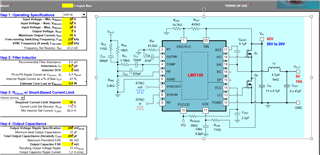
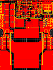
Hi friends. I started building a converter on the LM5146. But my efficiency is 5-10% lower than in the calculator. 

At an input voltage of 62 volt , Current  40 mA. Output voltage 5 V , this is without load. Frequency 230 KHz.
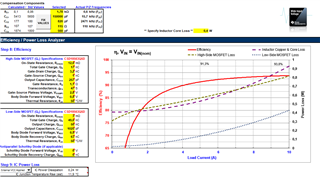
input voltage of 62 volt . Output voltage 5 V   . load 3.9 А    Converter efficiency 81.3 % 
input voltage of 62 volt . Output voltage 5 V   . load 7.8 А    Converter efficiency 85,8 %  

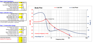
Both figures are 7% lower than indicated in the calculator. 
I use transistors High-Side CSD19534  ,  Low-Side CRSM038N10N4
Inductor  SMMS1770-4R7M .  
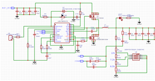
I am adding oscillograms. 
1. HO
2. LO
3. SW

How can I improve the efficiency? Is this normal operation of the converter?


  • Taras,

    Send on the completed quickstart calculator file (with the correct MOSFET parameters entered) as well as the schematic and layout. I notice you have a ton of ringing on the SW node voltage. Is it possible to use 80V instead of 100V FETs for better efficiency? Or use higher Rdson, lower capacitance device for the high side to reduce switching losses (given the low duty cycle).

    If Fsw = 230kHz, you can set the loop crossover at 30kHz (8kHz as shown is very slow). Also, why is the current limit set at 50A if full load is 10A? 15A should be fine.

    One option is to try your BOM on the LM5146 EVM, a known good layout.

    Regards,

    Tim

  • It is possible that the input voltage will rise to 80 volts, so I chose 100 volt transistors. 

    I used an online calculator to calculate the converter.WEBENCH® POWER DESIGNER  https://webench.ti.com/power-designer/switching-regulator/customize/53?VinMin=15&VinMax=75&O1V=12&O1I=20&base_pn=LM5146&AppType=None&Flavor=None&op_TA=30&origin=pf_panel&lang_chosen=en-US&optfactor=3&Topology=Buck&flavor=None&VoltageOption=None

    1. I entered the correct transistor specifications into the calculator.
    2.
    I don't really understand how crossover frequency works, so I used the values ​​from an online calculator.
    3.The current limit also used a value I got from an online calculator.
    I am attaching a file with the correctly specified transistor parameters.
    3022.LM25145_quickstart_calculator_A5.xlsm


  • Hi Taras,

    Are you still using CRSM038N10N4 for the low-side FET? This has unnecessarily low Rdson for a 10A load and extremely high capacitance and Qrr. The high Qrr of 120nC is contributing to the noisy waveforms and low efficiency. Consider using one of the FETs specified for the LM5146 EVM or similar FETs. Update the FET parameters in the quickstart as needed to see the efficiency.

    50A is too high for the current limit - the inductor will saturate. Also, just set the crossover at 10% of Fsw - that's always a good starting point.

    PS: as an alternative here, you could consider the LM70880 80V, 8A converter (or if 10A is absolutely required, then two LM70860 80V, 6A converters in parallel). These are converters with integrated FETs, and as such so much easier to implement than a controller with external FETs.

    --

    Tim

  • Thanks, I understand, I'll try to buy different transistors. But I'm continuing to experiment with the converter.

    The value of 50A was given to me by the calculator and not by checking. But I can change this by replacing the resistor.

    I also don't quite understand how to use the values. How do I choose the right value? Fz1, Fz2, Fp1,Fp2.

  • Follow the quickstart calculator for compensation values – just ensure that Cout and its ESR are accurately characterized (i.e. derate ceramic cap value for voltage).

  • I replaced the transistors today. Installed CSD18563Q5A. The efficiency increased by a few percent. But it is 3-5 percent lower than what the calculator claims. Also, the ringing on the SW contact did not disappear, but remained as it was.

  • See app note SNVA803 for correct input cap placement to alleviate ringing. Layout is critical.