This thread has been locked.

If you have a related question, please click the "Ask a related question" button in the top right corner. The newly created question will be automatically linked to this question.

UCC28951: Excessive MOSFET Heating in a PSFB Converter with Current Doubler Topology Using UCC28951PWR

Part Number: UCC28951

Tool/software:

Hello everyone,

I am designing a PSFB converter with a current doubler topology in the rectification stage, using the UCC28951PWR controller. For the rest of the circuit, I am following the topology from the datasheet, where the drivers and the controller are referenced to the secondary ground and the full-bridge MOSFETs are driven through gate drive transformers.

The issue I am encountering is that the full-bridge MOSFETs heat up excessively, quickly reaching 90°C with just one minute of operation and a load of 3 A. Initially, I considered two possible causes:

  • The high-side and low-side MOSFETs might be short-circuiting.
  • The gate drive might not be fast enough or there could be an issue with the turn-on process.

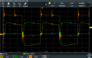
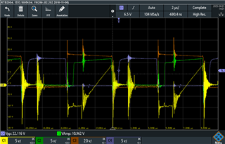
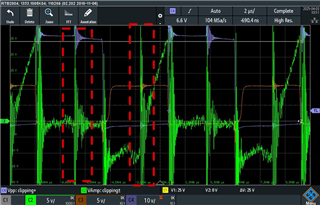
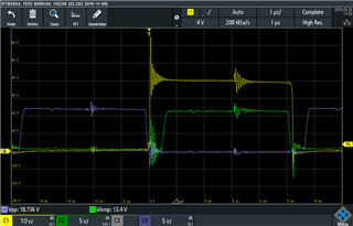
I have ruled out these hypotheses by analyzing the following signals in the lagging and leading leg:

  • Blue: Voltage at the low-side MOSFET gate.
  • Green: Voltage at the high-side MOSFET gate.
  • Yellow: Voltage at the intermediate node of the branch.

As shown, there is no crossing between the gate signals. Moreover, the waveform indicates that this branch is performing soft switching. First, the low-side MOSFET gate is turned off, and shortly afterward the voltage at the intermediate node changes from 0 to Vin. If I am not mistaken, this behavior is due to the shim inductor forcing the continuity of current, which causes the low-side MOSFET’s capacitance to charge and the high-side’s to discharge. After this process, the high-side MOSFET gate is activated (with ZVS already achieved), and finally, the high-side MOSFET is also turned off under ZVS conditions.

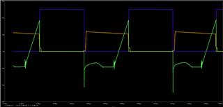
I am attaching the corresponding images for the lagging leg and the leading leg, as well as an image showing the MOSFETs heating up:

Image of the lagging leg


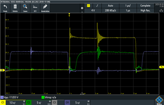
Image of the leading leg

Heating of the mosfets

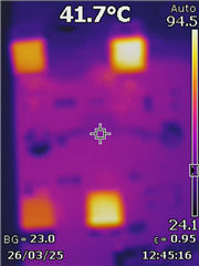
(Lagging leg-Right side / Leading leg-Left side)

Although the previous first two images show considerable noise, I performed a test where I connected together the primary and secondary grounds, driving the low-side MOSFETs directly from the driver. For the high-side MOSFETs, I still used the gate drive transformers to generate the 12V from its source to gate. In this test, the noise observed in the high-side MOSFETs was almost negligible, yet the heating persisted.

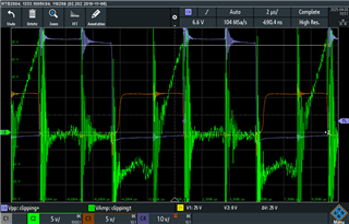
Finally, I used two half-bridge drivers to drive the MOSFET gates directly, bypassing the transformers. This way, I ruled out that the problem was caused by the gate drive transformers, as well as the possibility that the noise was due to a layout issue (since in this case the traces are “flying”). However, the result remained the same.

I believe I may be overlooking some important or fundamental detail in the design. Has anyone faced a similar problem or could suggest any clues to help identify the cause of the overheating?

Thank you very much in advance

  • The dead time between high and low side seems to be high for me. You mentioned that you managed to get waveforms with much lower noise/ringing. Can you share that instead?

    Why do you think the temperature is too high? Do you have any reference to show much lower temperature?

  • Dear Ning,

    Thank you for your response.

    Indeed, the dead time seems quite high, and both legs appear to be achieving ZVS, which by the way I find unusual given that the load was only 3A and the shim inductor was minimal (220nH).

    Regarding the waveforms you requested, I have attached a screenshot below.

    As I mentioned earlier, I conducted a test where I connected the primary and secondary grounds together, driving the low-side MOSFETs directly from the driver. For the high-side MOSFETs, I continued using gate drive transformers to generate the 12V from source to gate. In this test, the noise observed in the high-side MOSFETs (yellow trace) was almost negligible, yet the heating issue persisted.

    Due to this setup, the low-side MOSFET gate voltage only swings from 0 to 12V, while the high-side MOSFET gate voltage varies from -12V to 12V since it is driven through the gate transformer.

    The following image represents the waveforms of the leading leg MOSFETs:

    • Orange: Voltage at the intermediate node of the branch.
    • Green: Voltage at the low-side MOSFET gate.
    • Yellow: Voltage at the high-side MOSFET gate.

    As seen in the waveforms, the MOSFET directly driven by the low-side driver exhibits significantly more ringing compared to the one driven through the transformer. However, the ringing in the high-side MOSFET remains below 2V at all times, meaning it is insufficient to turn it on.

    Regarding your question, "Why do you think the temperature is too high?"—I believe the issue is not with how the FET gates are driven but could be related to the body diode. There may be unwanted currents passing through it, or possibly reverse recovery effects causing excessive heating.

    Until now, I have only been monitoring the MOSFET gate voltages, which do not reveal everything. If abnormal current is flowing through the body diode, it may be hidden from my observations. To gain better insight, I placed a shunt resistor in series with the high-side MOSFET of the leading leg to monitor the current flow for any irregularities.

    The following image shows:

    • Yellow: Current through the MOSFET.
    • Green: High-side MOSFET gate voltage.
    • Orange: Voltage at the intermediate node of the branch.
    • Blue: Low-side MOSFET gate voltage.

    For comparison, I have also included a simulation under similar conditions.


    Additionally, I want to emphasize that I am using a current doubler topology for rectification. At the time, I verified that this controller should be compatible with this topology, even though it is not the one shown in the datasheet (which presents a full-wave rectification phase with a center-tapped transformer).

    However, since I am encountering an issue whose cause I have yet to identify, I need to consider the possibility of a conceptual error. Therefore, it would also be helpful to confirm whether my topology is indeed compatible with the UCC28951.

    I look forward to your feedback. Thank you very much.

  • Hello,


    Your inquiry has been received and will be answered in the order it was received.


    Regards

  • Hello, as an update:


    To obtain more information, a shunt resistor was placed in series with the low-side MOSFET of the leading branch to measure the current flow.

    The following waveforms were obtained from the measurement:

    • Yellow: Current through the upper shunt (A).

    • Green: Current through the lower shunt (A).

    • Orange: Gate voltage of the low-side MOSFET.

    • Blue: Voltage at the middle node.

    A very intense ringing has been identified at moments when the MOSFET channel is off. This indicates that current is flowing through the body diode, both in forward and reverse bias. Although these periods are in the nanosecond range, they could explain the heating that has been observed.

    The most concerning peaks coincide with the switching of the MOSFETs in the opposite branch, which is not shown in the oscilloscope capture. This suggests that the noise is being injected from one branch to the other.

    At present, the origin of this ringing is unclear. One hypothesis is that it may be related to the physical design of the assembly or the PCB layout.

    When comparing the experimental waveforms with a simulation of the same circuit under identical conditions, it was observed that, aside from the noise present in the real implementation, the current waveforms through the MOSFETs match.

    The theoretical circuit does not exhibit ringing, but it does appear in the physical implementation. Therefore, the issue could stem from the PCB design or the way the components are arranged.

    Additionally, the current paths in each switching cycle can be described as follows:

    • The current path during one half-cycle, which forms an almost closed loop.

    • The current path during the other half-cycle, which extends further, forming approximately one and a half loops.

    I am not sure if this could be the issue...

    Thanks in advance

  • Hello,


    Can you share a schematic for review?


    Regards,

  • Hello Mike, here is the requested schematic. Thank you

    Full Bridge.pdf

  • Hello,


    I reviewed the schematic and functionally it looks O.K.   I can see that you are trying to do the adaptive delay approach by having ADEL and ADELEF controlled by a resistor divider off the CS pin.  I would recommend a fixed delay approach it easier to setup the timing for this approach.  The following link will bring you to an application note that reviews the step by step design process of a phase shifted full bridge using the UCC28951.  There is a link to an excel design tool that uses the same equations in the design tool.  This application note even calculates the power dissipation of the components that you are using.  You can use these tools to help check and adjust your design.

    https://www.ti.com/lit/pdf/slua560


    I would first check the power dissipation of the FETs you are using and calculate the power dissipation that you can with excel tool mentioned above.  Then you the thermal impedance junction impedance junction to case to calculate how hot the surface of the case should be.   The surface temperature should be the ambient temperature plus the power dissipation time thermal impedance junction to case.  If this matches your test data than you use a lower Rdson FET and/or add heat sinking.


    If the design is running hotter than your calculations you might be hard switching the H Bridge FETs.  I would then set the output to 10 % load while using the fixed delay approach and setup your turn-on delays based on application note slua560.

    The other thing you might want to check is that your Out E and Out F timing is setup correctly.  If is not you could get excessive heating.  The application notes and excel tool mention above will guidance on setting up the delays for Out E and Out F.


    Regards,

  • Hello,

    Thank you for your response. I will try replacing the adaptive delay with a fixed value as you suggested.

    Regarding the Excel file you mentioned, I had already reviewed it. However, the topology shown there is different from mine, as I’m using a current doubler topology in the rectification stage.

    That said, I don’t believe the issue is related to the Rdson of the MOSFETs, since the problem appears even at just 3 A of output current — far below the 80 A the converter is designed to handle.

    As shown in the last three images I attached, significant current oscillations appear across the full-bridge MOSFETs while their channels are off. I suspect this is the source of the excessive heating. What I haven’t been able to determine is what’s causing these oscillations. They occur whenever any of the four FETs are turned off, and the voltage at the switching node shifts polarity (from 0 to Vin or vice versa). This shift is likely due to the charging and discharging of the parasitic capacitances in the MOSFET branch, driven by the current briefly sustained by the transformer’s leakage inductance. This rapid voltage change may be triggering oscillations, as the inductance in the current path resonates with other parasitic elements.

    If that’s the case, I’m unsure what changes I could make to the schematic to suppress these oscillations.

    Another possibility, in my opinion, is that since my simulations don’t show any ringing, this might be a PCB layout issue due to the reasons mentioned above. I am attaching a shceme of the current paths:

    • Current path during one half-cycle, red.

    • The current path during the other half-cycle, blue.

  • Hello,


    Your inquiry has been received and will be answered in the order it was received.


    Regards,

  • Hello,

    Maybe your SRs are not setup correctly.   I would use the DCM comparator to turn them off and just use the body diodes.  If it removes the heating issue on the H bridge then you need to revisit your SR connections and timing.

    Regards,