This thread has been locked.

If you have a related question, please click the "Ask a related question" button in the top right corner. The newly created question will be automatically linked to this question.

TPS1101: Negative Power (PoE -54V) MOSFET switch enable design discuss

Part Number: TPS1101
Other Parts Discussed in Thread: TS3A5018, TPS23881, , CSD18536KCS, LM7480

Tool/software:

Hi Sirs, 

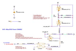
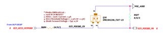
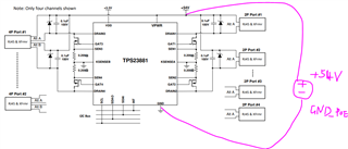
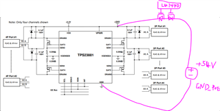
Current, I have an one power enable control design to asking as list, after will choice TI PMOS & NMOS combine solution ; but, not sure this idea is good or not?! 

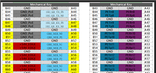
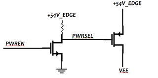
The project source will offer "-54V(negative)" power rail and possible setup off status for switch status(mean cut-off), then have external signal to control enable turn-on/off, 

Here is the my design example :  

[Noted : +54V_EDGE is equal to -54V(negative) power rail]

BRs

By Neil Chen

  • Neil,

    You should add a resistor between VEE and the PMOS.

    This is a common method to level shifting and inverting signals.  i don't see any issue with this plan.

    Regards,

    Chuck

  • Hi Chuck, 

    How about the VEE change to POEGND (0V) signal?! for my point, it's will not working to turn on successfully.

    Original idea for POEGND signal, adopt the TI.MUX/TS3A5018 to achieve switch on/off directly.... but extra consider the current reverse, the my leader think it's not a good idea. So, does you have any solution idea on here? Have any ref schematic can share it or not. 

    Hopeful, the VEE(negative voltage, -54V) and POEGND(0V) signals possible can use the same solution to switch turn on/off, whatever use chipset or MOSFET method. 

    BRs

    Neil

  • Neil,

    I am going to transfer this over to our POE team, it came to me by mistake and they are better to answer this question.

    Chuck

  • Hi Neil,

    Could your provide your PoE schematic? Thanks!

    Best regards,

    Diang

  • Hi Diang, 

    Let me clarify this question first, because I think it's not necessary offer relative PoE Schematic, if need you can take the TI.TPS23881 to be reference. 

    This question meanning, the gold-finger have customized define by ourself as snapshot; left-side is customized and the right-side is standard pinout. 

    Now, we adopt customize to doing relative design schematic but have plan to insert standard connector form-factor execute relative verification task in the future. That's why we must need use similar MOSFET switch/chipset to turn-on/-off signals, the main purpose is avoid signal short condition occur while insert standard connector. 

    Note : +54V_EDGE = negative -54V/ GND_POE : POE reference ground 

    So, do you have any relative similar design topic can share it?! Welcome we can brian-stroming to figure out on here, tks you!

    BRs

    Neil

  • Hi Diang, 

    After brain-stroming by myself, I offer my negative voltage (-54V_EDGE) and POEGND (ground) signals relative switch turn-on & off schematic on here, please help to review it and welcome if you have any comments. 

    In common, I think both enable switch on/off can enable successfully?! (for software control high/low) 

    1. -54V_EDGE (negative voltage) 

    2. POEGND (ground) 

    Above two schematic, please review it and many tks!

    BRs

    Neil

  • Hi Neil,

    Thanks for your reply. I will take a loot at your schematic and get back in 2-4 business days.

    Best regards,

    Diang

  • Hi Neil,

    May I assume your circuit like below? Could you mark at where you inject the TPS1101 circuit?

    Best regards,

    Diang

  • Hi Diang, 

    Yes, the +/- 54V circuit is like your snapshot drawing. 

    After you receive my latest design schematic before, can see the P-MOSFET will change to use N-MOSFET and choice TI.CSD18536KCS which can support up to 60V/Vds requirement. 

    Whatever -54V_EDGE or POEGND two signals, will implement the same N-MOSFET component to achieve switch turn-on/off. 

    Welcome if you have any review comments on here. 

    BRs

    Neil

  • TI is closed today, sorry about delay in response. 

  • Hi Neil,

    Thanks for your reply.  

    May I know if you want to have a bi-directional block circuit on the high-side with two FETs and a controller like LM7480? So you are able to oring the +/- 54V with another voltage source?

    Best regards,

    Diang

  • Hi Diang,

    Place two FETs actual reason as lists : 

    1. 1st FET/left-side purpose : the negative voltage turn-on switch to achieve bypass meaning, from S -->  D 

    2. 2nd FET/right-side purpose : avoid reverse current flow/voltage to cause this design route turn-on condition occur 

    Above all, that's why place two bi-directional FETs design on here. 

    In this case, we only expect negative voltage(-54V) & POEGND signals can turn-on switch FETs design, don't have positive voltage (> 0V) condition to insert. 

    Does you think both design schematic can reduce or not? Please let me know your idea on here, tks!!

    Best Regards 

    Neil

  • Hi Neil,

    Thanks for your reply. 

    Sorry that we do not have related PoE reference design. Ideal diode controller team may have related bi-directional circuit breaker.

    TI's PSE can be hold off by make the /reset pin low, which is more commonly applied to disable PSE. 

    But it is common in PoE circuit that bi-directional FETs are added for similar purpose, please make sure the capacitance value before and after the bi-directional FETs need to be carefully calculated. Normally the cap at the output side is much smaller than the power input side (10 x Cout < Cin normally, depends on application) , otherwise when FETs turning on the output cap needs very high inrush current that could cause overcurrent protection. 

    Hope above information can help and please let me know if you have further questions or concerns. 

    Best regards,

    Diang