


Other Parts Discussed in Thread: TPS543620
Tool/software:
Hello Team,
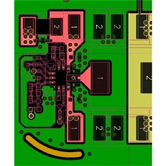
We found some TPS54360 PIN2, 5 and 3 crack issue on our board. So we are doing some layout investigation. Below picture is the example layout in our D/S and we got some questions.
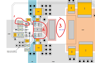
1. For circle1, the trace from "L" pin is 45deg to horizontal routing out, is there any special consideration to do this? Or is it must have?
2. On the device left the trace width is small than pin width, and on the right the race width is more wide than pin width. Is this due to current flow design requirement?
3. For circle 3, the bottom of the inductor is blanked, any specific reasons?
4. For the below our board layout, is there any specific issues which could cause the pin crack:
5. For the device pin1 and 5, we assume it will be better mechanical design to have square pin instead of "L" pin. Any specific reason to design "L" pin?
Best,
Qiang
