This thread has been locked.

If you have a related question, please click the "Ask a related question" button in the top right corner. The newly created question will be automatically linked to this question.

TPS54200: Inquiry regarding TPS54200 defect

Part Number: TPS54200

Tool/software:

Hi, TI expert

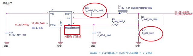
The customer's product has TPS54200 applied, and there are the following defect issues.

- There have been 4 defects so far where REG's GND (1pin) and PWM (5pin) are short-circuited, and all of them have been confirmed to have a burnt phenomenon at the same point as a result of de-cap.

- The customer is continuously trying to reproduce the same defect, but is unable to reproduce it, so he inquired whether it is technically possible to confirm.

TPS54200_DECAP.zip

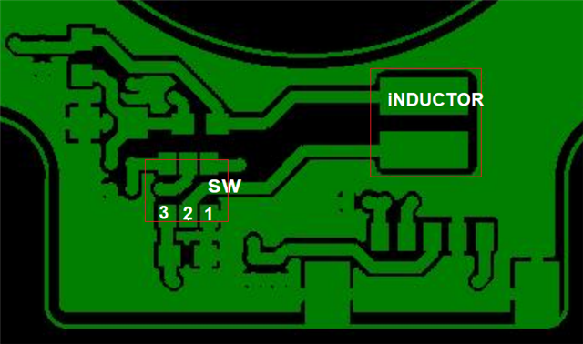
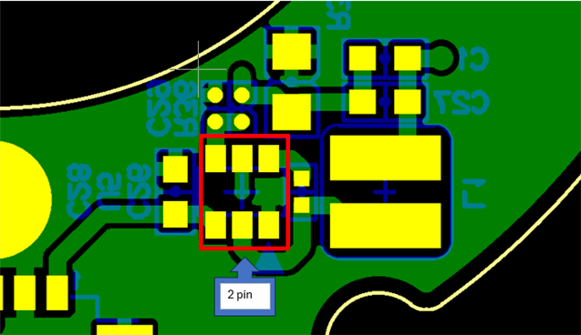
Can you tell me which pin was damaged in the attached de-cap photo?

Can you share if TI has a history of CQE (defect analysis) for the same defect?

Please check. Thank you.

  • Hi Grady,

    How many TPS54200 customer had used?  

    Can you upload the circuit schematic and PCB layout for checking?

  • Hi, Andy Chen

    This is an item that has been used continuously for a long time, and on average, more than 300K is used per year.

    It is said that the same defects occur on average in about 1% of production every year.

    I am attaching the circuit diagram and PCB layout below.

    4617.PCB Layout.pdf

    Please check. Thank you.

  • Hi Grady,

    Our expert will give you feedback later.

  • Hi,

    The Cin cap placement is good, but its voltage rating should be 25V or higher.

    The SW trace was not routed properly, it should not be placed under the IC package as its strong noise may impact normal operating. 

  • Hi, Andy Chen

    According to what we have confirmed with customers, there were defects on boards where the SW pattern passes under the IC, but there were also cases where the same defect occurred on boards where the SW pattern does not pass under the IC, as shown in the captured screen below.

    In this case, the same defect symptoms occurred, so if there are any other causes of the defect, please give us your additional opinions.

    Please check. Thank you.

  • Hi,

    On above layout, the Pin1 GND trace was not routed properly which maybe even worse than the SW trace under the IC !

    TPS54200 is a buck converter which require the input cap must be placed very close to VIN and GND pin, otherwise the trace parasitic inductor may generate high spike noise during switching transition, it may cause unstable switching or even EOS damage at high Vin condition.