This thread has been locked.

If you have a related question, please click the "Ask a related question" button in the top right corner. The newly created question will be automatically linked to this question.

TPS25980: E-fuse power up issues

Part Number: TPS25980

Tool/software:

Hi,

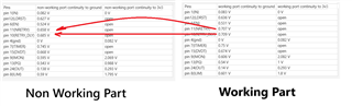
I have used 32 pcs of TPS259802ONRGER device in my design. The circuit used at each of the 32 locations is identical. Upon testing I found that only 6 out of the 32 devices are powering up.

Since the circuit is identical at all locations, it is obvious that my PCB has some assembly/soldering issues. Upon visual inspection, I did not find any soldering issues for the failing devices.

I have verified that none of the non-power/non-ground pins on the devices are shorted to ground. I know that the input power and ground pins are soldered correctly, since I can seen activity on the ITIMER pin when the device gets enabled. 

I also know that there is no Overcurrent(OC) or Circuit-breaker(CB) event, since I do not see TIMER capacitor discharge. Also, I have measured the output impedance to GND and it shows 210 ohms as I expect it to be.

I have attached a file showing the waveforms that I have captured on the faulty circuit.

Can someone look at these waveforms and suggest what kind of assembly/soldering defect may cause this issue?

The fault seems to be occurring immediately after the device EN pin is pulled high simultaneous to IN pin applied with 3.3V.  

Maybe if some pins are open (not soldered), this issue may arise.

Thanks,

Ramesh 

TPS259802ONRGER_power_up_issue.pdf

  • I will get back to you on this by tomorrow i.e. 22nd May.

    Best Regards,
    Arush

  • Hi Ramesh,

    It looks like there is some noise or signal coupling with OUT, LDSTART, RTRY_DLY, ILIM, DVDT, IMON, NRTRY. 

    Can you check for the soldering by using diode mode of Multimeter and check for diode drop between GND (+ve) and device pins (-ve). We have some diodes which should show some diode drop for some pins. You can cross verify these readings with other device which is working fine.

    Best regards,
    Arush

  • Hi,
    Recently we have done diode measurements with a multimeter and concluded that all pins seem soldered correctly.
    Internal ESD diodes are detected in these measurements.
    I have attached a comparison of the diode measurements on working and non-working parts.
    I do not see significant differences in the diode drop, except on a few signals.

    The pins on all 4 sides of the IC are soldered correctly. But I dont have a way to check whether the thermal pads are soldered correctly.

    Thanks,
    Ramesh

  • Hi Ramesh,

    Yes, these readings looks fine. Is this issue happening on same board same sites over randomly at different sites for different boards? Did you also check with another device at same non-working site to verify if this follows board or device.

    Anyway to test this in isolation, i.e. disconnect the load and other board components and only turn on 1 site to check.

    Can you share layout (screen snip is also fine) for the non-working site

    Best Regards,
    Arush

  • Hi,

    I have built a total of 4 PCBs. This particular problem is observed only on one of the four PCBs. Attached picture shows the location of the 32 e-fuses on the PCB. Each efuse powers one OSFP network port. Blue ones show the working locations. Yellow ones show the non-working locations.

    I just want to state that this is not a design issue, since it works perfectly fine on 3 other PCBs.

    I was hoping you could look at the waveforms and tell us what type of failure it is by looking at the waveform signature.

    Can inadequate soldering of thermal pads cause this issue?

    Is there a way to check if the MOSFET inside the e-fuse is still good?

    Thanks,

    Ramesh

  • Hi Ramesh,

    Can inadequate soldering of thermal pads cause this issue?

    I don't expect this to cause this kind of issue as thermal pad is internally shorted to the Vin or GND pins.

    Is there a way to check if the MOSFET inside the e-fuse is still good?

    You are getting the ITIMER signal so that means the internal voltage rail is building up. To verify if the FET is fine or not is not very easy. Checking for IN to OUT short is one way but you have already done that. The dvdt is the gate of the FET and it is not building up so it doesn't look like the issue is in the FET.

    Best Regards,
    Arush

  • Hi Arush,

    Can you give some pointers on possible causes for this kind of failure (dvdt not rising)?

    I have already check that the pins of the IC are soldered.

    I have also checked that the external components are okay, including the dvdT capacitor.

    Thanks,

    Ramesh Srinivasan

  • Hi Ramesh,

    I am not how I can help here. Maybe you can check the currents to find if there is any unexpected current path.

    Best regards,
    Arush

  • Hi, 

    I did not see any current flowing through the device.

    I got some x-rays taken for the 26 non-working parts on the board. I have attached the x-ray plots.

    The x-rays do not show anything unusual, apart from some voids on the thermal pads.

    Can you check the x-ray images and provide your feedback?xray-analysis.pdf

    These x-rays are for the non-working devices on my board. Soon, I will get x-rays for the working devices also. I will upload them when available.

    Thanks,

    Ramesh Srinivasan

  • Hi,

    I have now attached the x-rays for the 6 working devices on my PCB. I did not see any difference in soldering quality between working and non-working devices. Any comments?

    Can I send some non-working devices to TI  for failure analysis?

    Thanks,

    Ramesh Srinivasan

    xray-analysis-working-devices.pdf

  • Hi Ramesh,

    For the Failure Analysis, you will have to get in touch with the Field guys supporting your org. 

    I believe the issue is not with the device as the fail rate is very high. The issue is more of a system level issue. 

    Are you based in Bangalore? Is it possible for anyone from your team to come to our office? That will ensure that we can check the board and the device both. I am on leave during next week but will be back on 5th July. Anyways the logistics to arrange this will also take time (gate passes for you and visitor permission for me)

    Let me know if you think this is a good idea.

    Best regards,
    Arush