This thread has been locked.

If you have a related question, please click the "Ask a related question" button in the top right corner. The newly created question will be automatically linked to this question.

BQ78350: BQ78350-R1+BQ7693003DBT+BQ76200

Part Number: BQ78350
Other Parts Discussed in Thread: BQ76200, BQ76930

Tool/software:

Hello!

How can we prevent the voltage supplied from the BQ7693003DBT to the BQ78350 from exceeding the specified range?

1. According to the datasheet of BQ7693003DBT, the nominal output of REGOUT is 3.3V, and the upper limit of the output is specified as 3.6V;

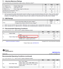
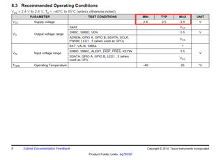
2.According to the datasheet of BQ78350, its VCC is specified to only allow 2.5V, with a maximum of 2.6V;

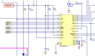
3.In one of my projects, I am using the BQ78350 + BQ76930 + BQ76200 solution. According to the schematic recommended by TI, the VCC of the BQ78350 is supplied by the REGOUT of the BQ76930.

In this case, the REGOUT of BQ76930 outputs 3.3V, which exceeds the electrical performance range of BQ78350's VCC. Could you help confirm whether this will cause adverse effects on BQ78350?


Thank you!

  • Hello,

    Yes, the REGOUT output of the BQ7693003DBT at 3.3V (with a maximum of 3.6V) exceeds the specified VCC range of the BQ78350, which is 2.5V nominal and 2.6V maximum. Supplying a voltage above the maximum rating can potentially damage the BQ78350, lead to unreliable operation, or cause long-term degradation.

    It seems like the Evaluation board schematic might have been created with a device whose LDO output was 2.5.
    In your case, you might need to step down the voltage. An easy approach would be to add series diode for voltage drop.
  • Hello, 

    In the specification of the BQ78350, I could only find the voltage range that SMBC/SMBD can withstand. I did not find the nominal voltage range that the SDA/SCL pins, which are used for communicating with the BQ76930, can withstand. Could you help me clarify the nominal voltage range that the SDA/SCL pins of the BQ78350 can withstand?

    Thanks!

  • Hello, 

    General purpose open-drain I/O pins,  – 0.3 V to 6.0 V 

    General purpose push-pull I/O pins,  –0.3 V to VREG25 + 0.3 V