This thread has been locked.

If you have a related question, please click the "Ask a related question" button in the top right corner. The newly created question will be automatically linked to this question.

LM706A0-Q1: Switch Node Reference Plane in IBB configuration

Part Number: LM706A0-Q1
Other Parts Discussed in Thread: LM706A0, LMQ61460, LM70880-Q1

Tool/software:

Hello Ti forum,

I would like to know what the reference plane is for the Switch Node when using the LM706A0-Q1 in IBB configuration.

1. Is the Switch Node referenced to the GND of the IC, which in the IBB case is -Vout.

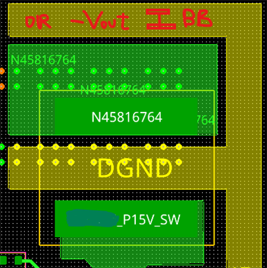
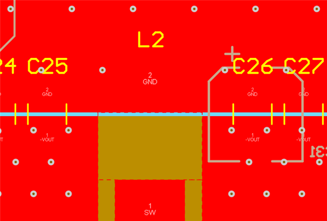
I am investigating the better layout when using a shielded inductor.

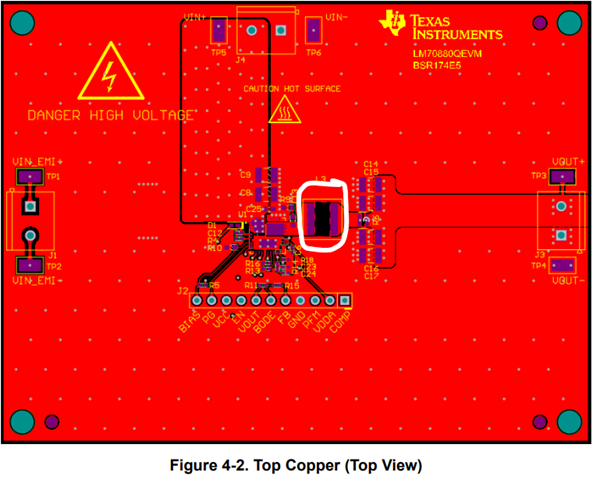
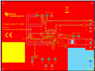
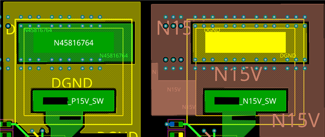
Application notes and design reviews, including LMQ61460 EVM, indicate to use the GND referenced copper pour directly under inductor, as well as a solid plane layer 2 for example also referenced to GND.

Now with the IBB case the IC GND reference is -Vout.

If the Switch Node is referenced to GND IC, should one apply the copper pour to -Vout?

It is understood that the current loops are different in the IBB case.

I am planning to apply the same copper pour directly under the inductor as well as a solid plane on the next layer down, same as in standard configuration.

This copper pour is referenced to -Vout, IBB Case, instead of GND in the normal case. An example of GND under Inductor is attached.

Please let me know your thoughts on this issue. 

Thanks,
David


  • Hi David,

    1. Is the Switch Node referenced to the GND of the IC, which in the IBB case is -Vout.

    Yes, that is correct. The SW node is reference to -VOUT.

    If the Switch Node is referenced to GND IC, should one apply the copper pour to -Vout?

    Yes, that is also correct.

    I am planning to apply the same copper pour directly under the inductor as well as a solid plane on the next layer down, same as in standard configuration.

    When I layout a board, I tend to not have any copper pour under the inductor to keep the noise from coupling to the GND plane. For IBB configuration, it will be -VOUT. See below for the LM70880-Q1 EVM as an example where I have circled in white.

    Ben

  • Hi Ben,

    Due to recent articles when using shielded inductors, it has been advised to use a copper pour under the inductor, including on the same layer. There is growing consensus on adding these copper pours as leakage currents are minimized when using shielded inductors, provided the manufacturers are accurate in reporting the shielding capabilities.

    In general, the eddy currents also cancel but not 100%. Eddy currents have been less of a factor when using shielded inductors.Hence, we are back where we started. What is the best approach? Note the following picture from TI.

    The LMQ61460 EVM does not remove the copper under the inductor on the same layer and has a solid ground plane on L2.

    I agree on the SW node -Vout reference plane, IBB configuration. I have a very high density pcb where space is premium. I would like to encapsulate the switching inductor reference node as in the example above. The only difference is that the plane reference is -Vout, the case shown is GND for the standard BB configuration.

    Any advice or insights are appreciated.

    Thank you,

    David

  • Hi David,

    In general, the eddy currents also cancel but not 100%. Eddy currents have been less of a factor when using shielded inductors.Hence, we are back where we started. What is the best approach? Note the following picture from TI.

    I am building an EVM that will be IBB specific and I have removed the pour under the inductor. The inductor that I am using is a molded version. I have also read that adding a copper pour under a shielded inductors will not have any effect on the inductance of the inductor. So the decision will be up to you if you want to add or not to add a copper pour under the inductor.

    As for the IBB EVM that I am building, I need to build an EVM that will work for all inductors. 

    Ben

  • Hi Ben,

    Your advice is greatly appreciated. Please let me know your thoughts as I show both examples.

    With BB configuration (LEFT SIDE) , I have seen designs with output inductor node encircled by GND, yellow. Layer 2 plane is Solid GND.

    With IBB configuration (RIGHT SIDE), I am uncertain if this is a valid or wise idea due to -Vout (N15V) is next to the switching node (N15V_SW) of the inductor, light brown.

    In IBB Config, the SW node is referenced to -Vout, should the plane, layer 2, under the N15V_SW be GND or -Vout (N15V)?

    These rails power some A2D circuits, and I would like to minimize noise.

    Any suggestions and insights are greatly appreciated. I am in final layout.

    Thanks,

    David

  • Hi David,

    I would choose the layout on the right where -VOUT is around the SW node. I would space the SW node from VOUT so the capacitive coupling is a little less. Below is a snippet of the IBB EVM that I am working on. As you can see, I don't encase GND with -VOUT but it may be different in your situation. 

    In this layout, the output capacitors are on the top side of the EVM.

    Ben

  • HI David,

    Just reaching out to you to ask if you have any other questions. If not, please close the thread by clicking on "resolved". Thanks!

    Ben

  • Hi David,

    Reaching out to you again. Please close the thread if there are no further questions. Thank you,

    Ben

  • Hi David,

    Are there any updates?

    Ben