


Other Parts Discussed in Thread: TPS25820, , TUSB1142
Tool/software:
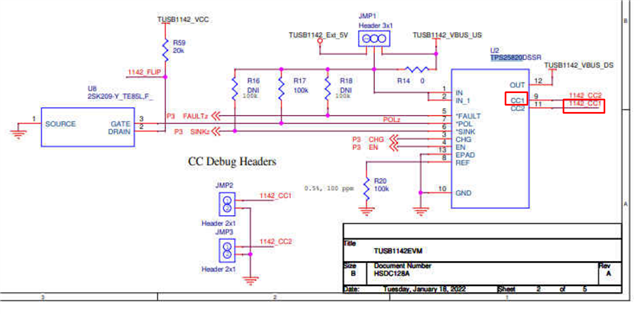
Hello,
Looking at the TUSB1142EVM schematics. Why does the CC1 pin of the TPS25820 have the 1142_CC2 net label and connect to the CC2 pin on the usb-c connector?
Doesn't the U8 FET already invert the *POL so that it matches up correctly with FLIP/SCL pin of the TUSB1142?
Thanks,
