Tool/software:
Hello,
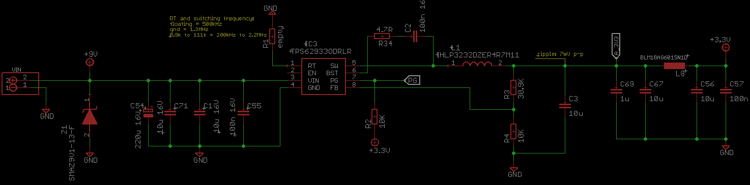
i'm designing a power supply around TPS62933O which would power an audio DSP and ADC/DAC converters. I've opted for the TPS62933O for its out-of-audio feature.
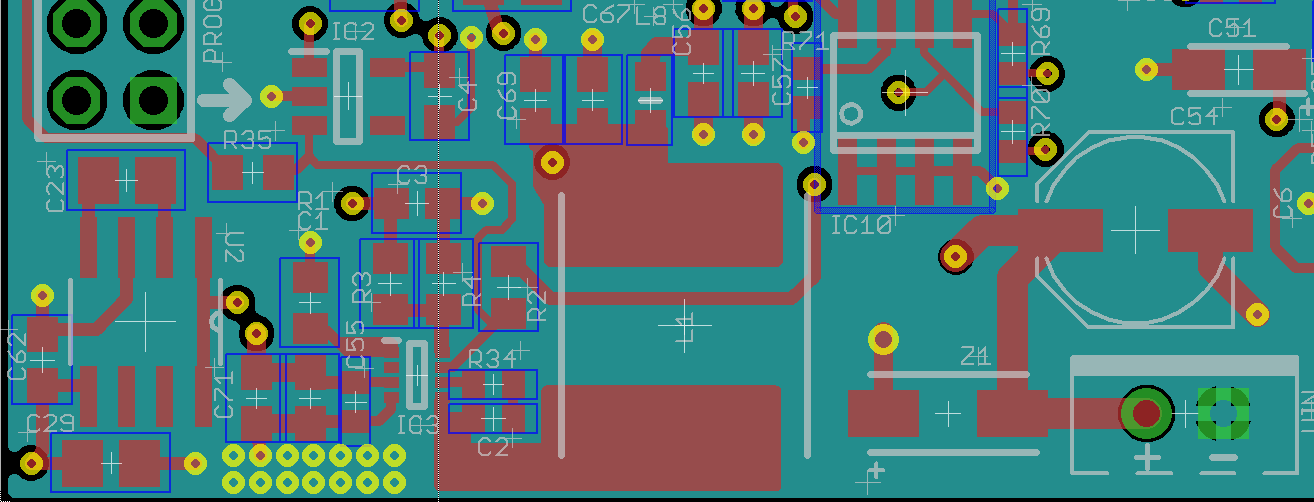
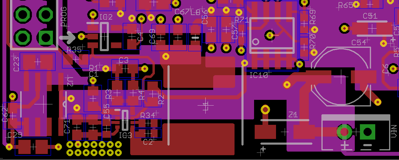
Can you check if i'm doing something wrong in my PCB layout and schematic?
I've used WEBENCH tool for the schematic and simulation and, as from datasheet suggestion, i've added a 4.7R resistor between C2 and BST pin. The resistor is rated for a power of 62.5mW, is the power rating ok for this resistor?
Input voltage is 9V, Output 3.3V, load would be around 400 to 600mA.
R1 is not fitted but i may experiment with different values or left floating.
The PG pin is used to trigger a reset supervisor ic.
The board is a 4-layer design, BOTTOM not showed since has no meaningful traces for the supply section.

TOP + GROUND PLANE:

TOP + POWER PLANE:
Thank you!
Omar