This thread has been locked.

If you have a related question, please click the "Ask a related question" button in the top right corner. The newly created question will be automatically linked to this question.

TPS1HC100-Q1: Building the circuit around the IC

Part Number: TPS1HC100-Q1

Tool/software:

1. Does the input voltage of DIAG_EN being 3.3V or 5V affect the operation of FLT? (In the datasheet, only the condition of VDIA_EN=5V is mentioned)

2. According to our current circuit, the maximum input voltage for the load connected to FLT is 3.6V, so FLT needs to use 3.3V as the pull-up voltage. Is this design reasonable? 

3. The specification document does not clarify the VOH/VOL characteristics of the output terminal (ILIM). Please provide relevant design information.

4. Regarding the design of GND, if we are not using as a primary power, relevant GND circuitry still required?

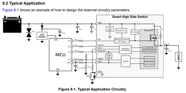
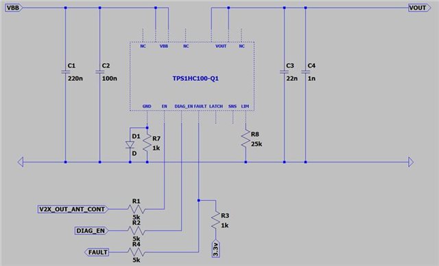
5. Below is the reference circuit diagram we designed; please help check if there are any issues.

6.What is the timing relationship between DIAG_EN and EN: during power-up, during fault, and during power-down?

Additional information:

1. Input voltage range: min 11.82V~typ 11.94V~max 12.06V;

2. Subsequent load: input voltage range: min 8.5V~typ 13.2V~max 16V; consumption current typ 0.5A~max 1A;

3. ILIM design values: min 1.2A~typ 1.7A~max 2.3A;

4. Required functions: OV, UV, ILIM (no need to monitor current value), FAULT feedback;

5. Input and output signal characteristics: 

EN: VIH:min 2.72V~max 3.39V;VIL:min 0V~max 0.68V; 

DIAG_EN: VIH:min 2.72V~max 3.39V;VIL:min 0V~max 0.68V;

FAULT(designed output value): VFLT_H type 3.3V,max 3.6V

Thank you for your help.

  • Hello, 

    I am working through your questions. I should have a response on Monday Dallas time. 

    BR, 

    Alan

  • Hello,

    May I ask if there is an answer now?

    Zhao

  • Hey Zhao, 

    1. Voltage of DIAG_EN does not affect the operation of FLT as long as the voltage level is higher than the Input voltage high-level

    2. 3.3V PU is acceptable on FLT

    3.  I don't have data available for VOH/VOL for ILIM. The application case would be the external resistor to IC_GND. Let me know if more information is needed here in addition to the purpose. 

    4. The GND network is recommended for reverse current protection and protection from loss of power supply. This external circuitry is recommended in every application.

    5. In section 8.1 the datasheet has a typical application example. Looking at your schematic the main issues I see are with the ILIM GND connection. It should be routed to IC_GND.

    6. All timing information is available in the switching characteristics as well as the SNS timing table. The deglitch for each fault is available in Table 7-3. 

    BR, 

    Alan