


Tool/software:
Hi,
Below is my design setting
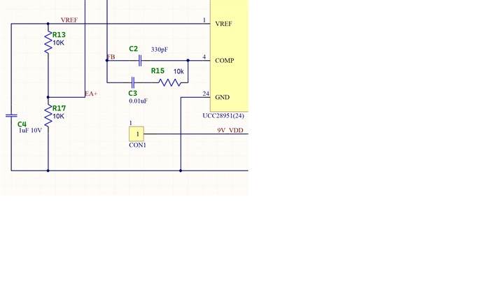
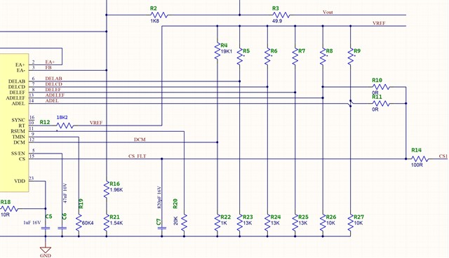
Vin min=35V, Vin max 60V, Vout 4V/130A, Fsw: 300kHz, center tapped transformer PQ3235 core, 45uH, 5:1:1T, turn ratio 5, leakage inuctance: 1uH. No Shin Inductor, Vin cao: 1066uF, Cout: 5800uF E cap, 22uF*20pcs ceramic cap, Current transformer 100: 1, 2mH, current sense resistor 8ohm.
output use STPS40120CT rectifier for simplication. My primary mosfet is magnachip MDU10N070MDU10N070RH_Preliminary_datasheet_ver0.0_20170222 0.185.pdf
At Vin 30V/Vout no load, vout is stable 4V, PWM outputs of UCC28951 is less noisy.
At Vin 40V/Vout no load, vout is unstable, oscillation between 4V to 4.2V, PWM outputs of UCC28951 is noisy.
When increase loading current from 0A to 0.1A, primary mosfet driver is damaged.
At Vin 40V/Vout no load, vout is unstable, even i change DELAB & DELCD from 10K to 33Kohm & change comp pin C3, add shin inductor 0.1uH etc
Except Vin=30V will lead Vout more stable. At Vin 40V/Vout no load, when i using x10 proble at DS & GSpin of leading leg low side mosfet, differential probe at
DS pin of leading leg high side mosfet, vout can be more stable at 4V, , PWM outputs of UCC28951 is less noisy. Iout can increase to >10A
However, At Vin 40V/Vout no load, when i using x10 proble at DS & GSpin of laging leg low side mosfet, differential probe at
DS pin of laging leg high side mosfet, vout become unstable again (oscillation between 4V to 4.2V) , PWM outputs of UCC28951 is noisy.
This Vin high issue will also affect in medium loading current, using x10 proble at DS & GSpin of leading leg low side mosfet, differential probe at
DS pin of leading leg high side mosfet, when Vout 4V, >10A lout, Vin rise from 40 to 45V, gate driver will also be damaged.
If this issue can not solved, i can not verify 4 PWM output together in same CRO screen together when Iout increase from no load.
Could you tell me the root cause and solution?
Thanks a lot
