Other Parts Discussed in Thread: BQSTUDIO, BQ40Z50, EV2400
Tool/software:
We are currently developing a Battery Management System (BMS) using the BQ40Z50-R2 IC, with SMBus communication for interfacing with BQStudio. The battery pack configuration is 14.8 V, 6600 mAh (4S3P).
We are facing an issue where SMBus communication is unable to establish a connection with BQStudio. The attached screenshot shows the error message encountered.
During PCB-level diagnostics, the following measurements were recorded:
-Voltage between PACK+ and GND: 0 V (expected: ~14–16 V).
-Voltage at CHG (Pin 31) and DSG (Pin 28): 0 V (expected: ~25.95 V).
-Voltage across R20 and at Q3: 0 V (expected: ~14.48 V).
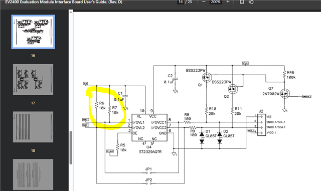
For reference, the schematic is attached.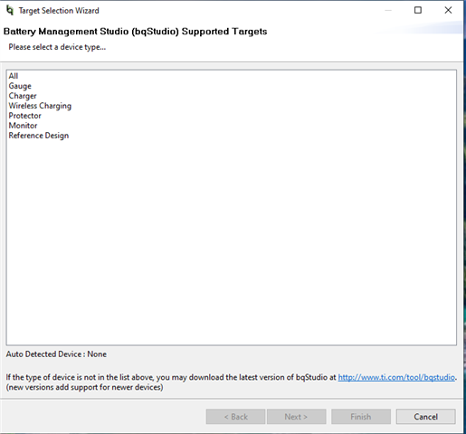
2046.0043-08-7081 sch.pdf