Tool/software:
Hi TI Team,
I have two requirements for a power supply design and would like your guidance:
-
72–120 V → 12 V, 2 W converter (Flyback or any easily isolated converter topology).
-
400–800 V → 12 V, 2–5 W converter.
I would like to clarify the following points:
A. Can I use this flyback control IC for both designs? If not, could you please suggest suitable alternatives?
B. If I want to commonize both designs on a single PCB, is it possible by changing only the transformer (turns ratio), or are there other major changes I should take into account?
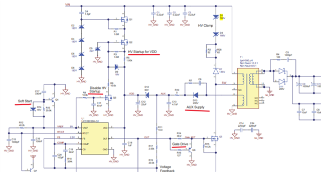
C. I need to understand the high-voltage startup for VDD. Specifically:
-
Why are two N-MOSFETs used and how are they controlled?
-
How is the controller’s VDD voltage maintained during operation — is it always supplied from the auxiliary winding or can it be sustained from VIN?
D. Could you also explain the role of the leading-edge blanking (LEB) circuit used in this schematic?
Thank You!