UCC28C59-Q1: Help Required with Design Trouble shooting

Part Number: UCC28C59-Q1

Tool/software:

Hi Team,
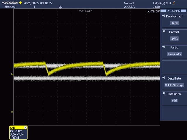
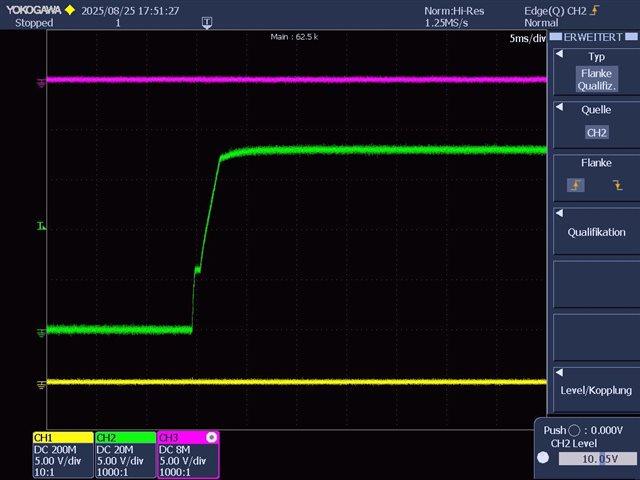
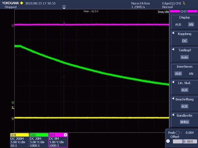
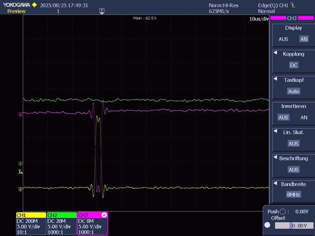
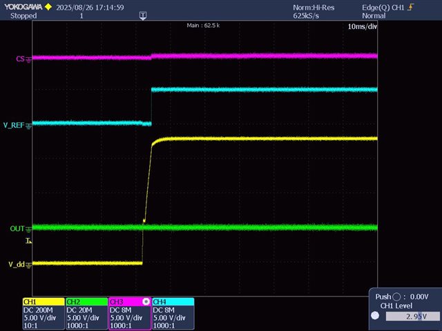
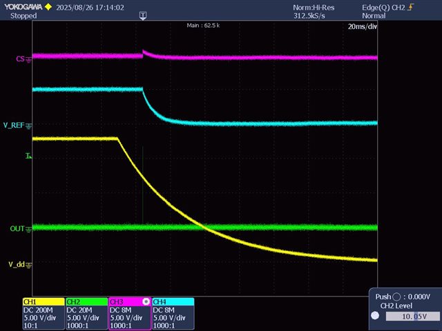
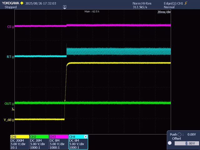
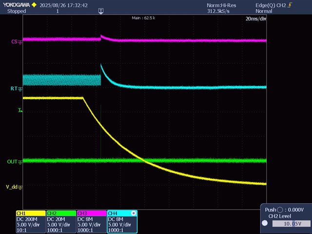
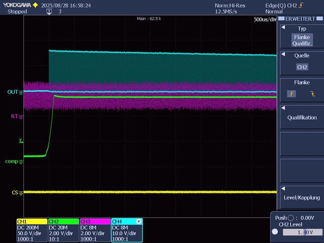
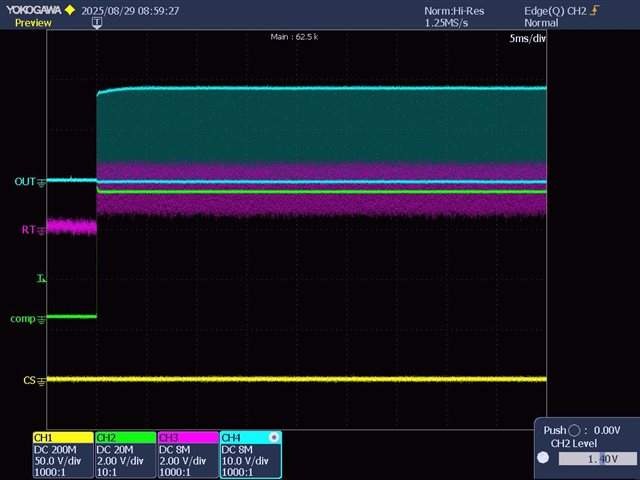
I designed an isolated dc dc flyback converter using Webench. I designed the PCB keeping in view the layout guidelines. Now after assembly, when i power up the board, i do not get anything at the output. After basic troubleshooting, i found out that the IC is not working. I saw that one of the reasons was that the VDD pin voltage remains 11V with 24V input supply. I increased the input voltage upto 32V which in turns increases the VDD pin voltage upto 15V but still the ic does not turn on and generate any signal for switching the MOSFET. The only other signal i could see was voltage on FB pin which is around 2V or a little above. Can someone guide how to go about this problem. Is there a problem with the design from the Webench or some other issue that i need to take care of? I am attaching the webench design report alongwith the schematics.  
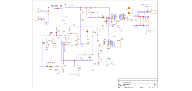
Isolated_Flyback_CC.pdf

  • Hi,

    I suspect C13 = 33uF takes long soft start time so C8 cannot be charged up from aux then VDD drops to UVLO off. You can try reduce C13 to 0.1uF to see if ok to start.

    You can monitor VDD pin voltage waveform to help debug.

  • Hi Hong,

    I changed the C13 to 0.1uF as suggested and still no difference. This is the behavior on the VDD pin. It stays constant around 11V as shown in image by white line. Then once i start increasing the input voltage it goes upto a value of around 15.5V. Once the value on the input goes beyond 33V, the voltage on Vdd starts decaying and charging keeping it below the UVLO and not turning on the IC. 

  • Hi,

    What is D5 clamping voltage value? Is D5 clamping at about 15V?

    What is the yellow waveform?

  • Hi Hong,

    The clamping voltage of D5 is 22V. The yellow waveform is of Vdd pin.

  • Hi,

    Both white and yellow are VDD based on your message -  but they are not the same. Please explain.

    UCC28C59-Q1 needs 17.2V to start. It looks VDD on UVLO on and off.

    Can you change R1 and R4 to zero then setup VIN =18V to see if you can get OUT pin with pulses?

  • Hi Hong,

    Yes all the waveforms were from Vdd pin. I just saved the behavior under different VIN (24V, 32V and 34V). When i increased VIN, VDD voltage improved but ultimately started showing sawtooth which is shown in yellow. 
    On your second suggestion, i removed the R1 and R4 and gave 18V on the VIN. I see that the VDD pin rises to 18V but i couldn't see any output pulses. But when i turn off the VIN, the IC outputs two 5usec pulses randomly approx of 13V amplitude as shown below. then i also see small voltage across the auxiliary winding of the transformer. But the problem persists that the IC does not turn ON at all. It should give some output pulses at least when VDD crosses 17.2V.


    VDD= (in Green), OUT= in Yellow, Aux winding = in Pink


    (Close up on out pulse)

  • Hi,

    I suggested to make R1 and R4 to zero, and change Vin = 18V to try. It looks you did this while the IC did not make pulses. I suggest you to change the IC to a new unit. Then re-do this with waveforms of OUT, CS, VDD, and VREF.

  • Hi Hong,

    I tried it with different ICs as suggested and It's the same behavior. No output pulses at the start and then a random output pulse during the turn off of the IC. Here are the waveforms during turn ON and turn OFF of the ICs.
    Waveforms during Turn ON

    Waveforms During Turn OFF

  • Hi,

    Please provide VDD, RT/CT, CS and OUT pin waveform when VDD = 18V.

  • Hi Hong,

    Here are the waveforms during turn On and off.

    Waveforms during turn ON


    Waveforms during turn OFF

  • Hi,

    It looks your circuit has connection something wrong. Re-try open pin 6 OUT (remove R11) and remove Q1 and Q2. I think you need to change to a new IC as the IC could be damaged due to some connection not correctly. 

    Remove R11, Q1 and Q2, use a new IC, then set up VDD = 18V, measure RT/CT, OUT, CS and COMP waveforms.

  • Hi Hong,

    I removed the R11, Q1 and Q2 components as suggested and was finally able to get some output waveforms. Here are the images:

    Waveforms during turn ON

    a close-up view

    Waveforms during Turn Off

  • Hi,

    COMP pin voltage needs to be high enough to make OUT pin pulses show. Typically COMP pin voltage needs 1.5V or higher.

    Your waveforms show something pulling COMP voltage low. You can open COMP pin to re-test. Then add back circuit one at time to see which pulling COMP low to prevent from producing pulses.

  • Hi Hong,

    I lifted the COMP pin of the IC and and even now it stays to low (around 300mV). Earlier it was giving some output at the start and the end but now, it just gives some waveforms on the output during turn off when COMP pin jumps to 5V for short time and nothing during turn on. Here are the waveforms of the behavior.

    Waveforms during turn on


    Waveforms during turn off

  • Hi,

    You can short FB pin GND to try. If COMP still not rising then the ic is dead then you need to change to a new IC.

  • Hi Hong,

    When i short the FB pin to the GND, the COMP does rise to 5V and IC outputs the waveforms continuously. Does this mean i have a problem with my feedback loop?

  • Hi,

    Yes you need to find why FB voltage is at that value which I guess > 2.5V to push down COMP < 1V then no pulses.