Tool/software:
Hello,
I am currently working on a design based on the TPS563200 buck converter, and I would kindly like to request a review of both my schematic and PCB layout.
Here is a summary of my design parameters:
- Input Voltage Range : 8.4V-6V (2S Li-ion cell)
- Output Voltage : 5V
- Output current : Max 2A
Schematic screenshot :

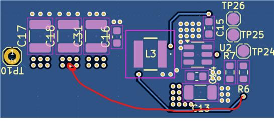
Layout TOP screenshot :
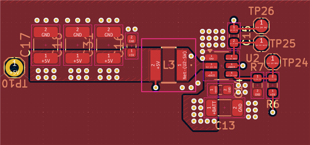
Layout BOTTOM screenshot :
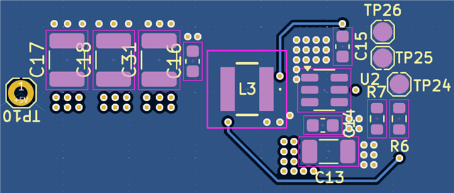
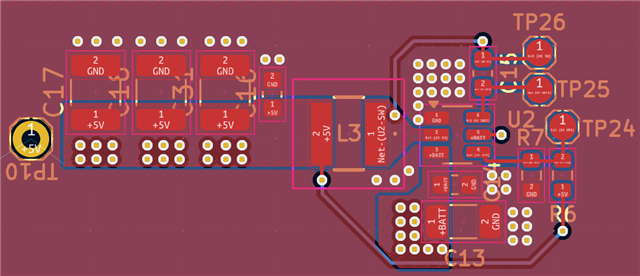
Layout TOP + BOTTOM screenshot :
The PCB layout is mainly inspired by Version 3 of application note SLVA922, but I would like to confirm that my implementation follows the best practices.
Thank you very much in advance for your help and support!
Best regards,
Thomas