Tool/software:
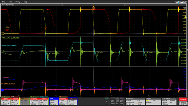
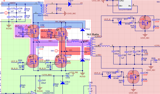
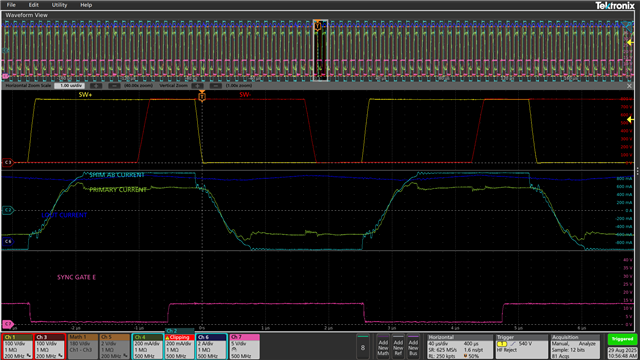
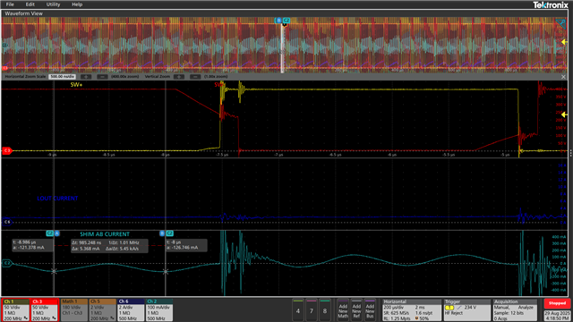
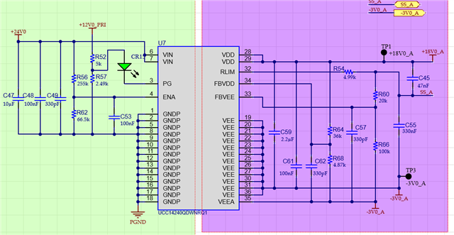
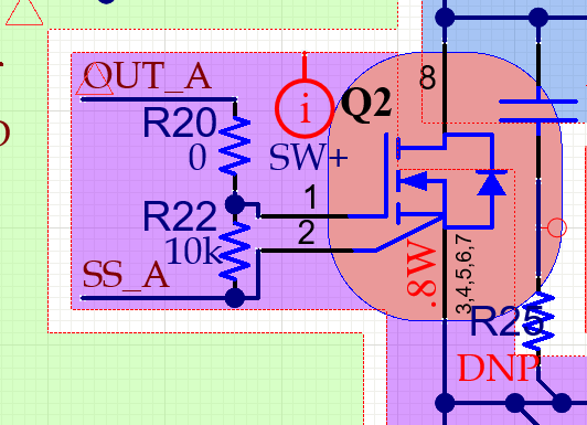
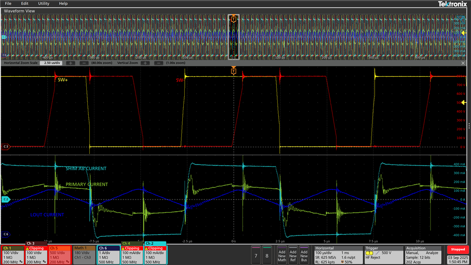
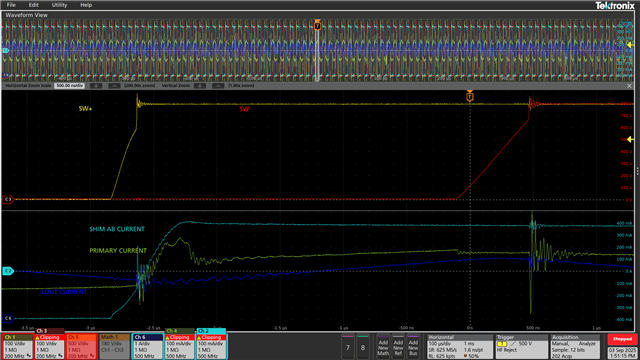
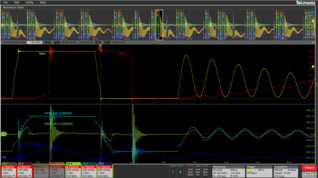
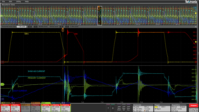
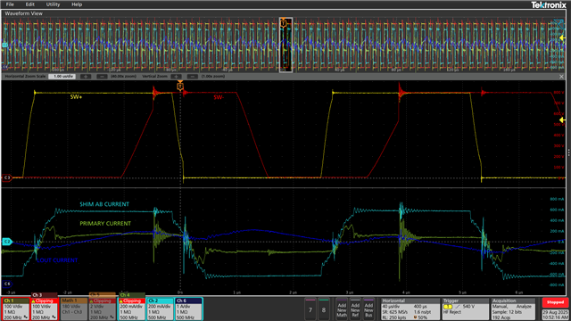
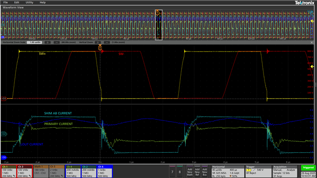
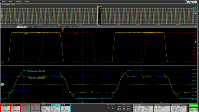
I have a design for a 200W, 800V to 12V converter using the UCC28950. I have used this controller on many designs. Previous designs were operating off of a 400V input bus and ranged from 100W up to 5kW. I've also used this controller to provide output voltages anywhere from 12V up to 96V output. In this design the resonant transitions are acting very strangely. The AB node and CD node resonant legs seem to operate in the exact opposite manner. The AB node has a much higher transition time and will resonate to the rails at a significantly lower load current. The CD node has a 'ramp rate' that is about 10x slower than the AB leg. The schematic is shown below and is the typical connection and layout from all previously used designs. I have captured waveforms showing this behavior. In the scope capture "SW+" is the AB Node, "SW-" is the CD node. I have the output inductor current, sync E drain voltage and the sync E gate captured as well. The First scope capture is at 800Vin and 1A Load. The second capture is at 800Vin and 8A Load. The third scope capture was installing a much smaller 25uH shim inductor. The AB node and CD node just have such drastically different ramp rates. Extending the CD leg delay time much longer than the AB delay optimizes this behavior, but it doesn't seem correct. I'm not so much concerned about the high ringing in these scope captures. The probing is very noise prone and the hard switching doesn't help. Once ZVS is achieved at the higher loads the majority of this ringing evaporates.
I'm very confused. From my understanding the energy that is stored in the shim current as well as the primary current both contribute to the resonance of the CD leg and from nearly every resource that I could find the AB node should be 'harder' to resonate than the CD node. What could be the cause of this behavior?
Due to the large Vin to Vout, the transformer turns ratio is about 28:1. The Primary inductance is about 35mH and I've tried to measure the leakages. I've seen about 100-200uH of leakage inductance and about 30pF of winding capacitance. My primary Bridge FET's are SiC and have about 10pF of Coss (pretty surprising!). The Sync FET's are lower voltage silicon fets and have about 450pF Coss. I have tried to eliminate every source of parasitic capacitance in my PCB layout with no significant effect on the resonant legs. I have constructed 3 different transformers attempting to alter the leakage inductance and capacitance. Different transformers affect the resonant transitions, but in all cases the CD leg always is far behind the AB leg. I have also experimented with different shim inductance values ranging from 25uH to 600uH. Again, the resonance exhibits the same 'backwards' behavior.
A second thing that I don't understand is how the shim current is so much higher in current than the primary current. In past experience I've seen this behavior but never fully understood the cause. From one perspective I feel that the leakage current spike on the front end of the power transfer stage rises to produce this current, but at heavier loads, this leading spike is much lower than the shim's current.